System and method for lithography simulation

a lithography simulation and system technology, applied in the field of system and method for lithography simulation, can solve the problems of limiting the diffraction range of the projection optics, affecting the lithography simulation effect, and the b>18/b> mask may not be “perfect”, so as to accelerate the lithography simulation, the effect of characterization, evaluation of the effect and/or interaction, and inspection of the optical characteristics and/or properties

Active Publication Date: 2005-04-07
ASML NETHERLANDS BV
View PDF55 Cites 188 Cited by
  • Summary
  • Abstract
  • Description
  • Claims
  • Application Information

AI Technical Summary

Benefits of technology

[0019] There are many inventions described and illustrated herein. In one aspect, the present invention is a system and method that accelerates lithography simulation, inspection, characterization and / or evaluation of the optical characteristics and / or properties, as well as the effects and / or interactions of lithographic systems and processing techniques. In a first principal aspect, the present invention is a system and method for simulating a lithographic design comprised of a plurality of polygons (which may or may not include resolution enhancement technology(ies)) arranged in a predetermined configuration. The system of this aspect of the invention comprises a microprocessor subsystem to convert the plurality of polygons to a pixel-based bitmap representation thereof (for example, a multi-level image such as 2, 4, 8, . . . 64, 128, 256 or gray-level). The pixel-based bitmap includes pixel data, wherein each pixel datum represents a pixel having a predetermined pixel size.

Problems solved by technology

Notably, mask 18 may not be “perfect”, due to its own manufacturing process.
Due to the wavelength of light being finite, and current techniques employing wavelengths that are larger than the minimum linewidth that is printed on wafer 22, there are typically significant light interference and diffractions during the imaging process.
The projection optics may be diffraction-limited.
However, lens subsystem 16c in the projection optics is most often not completely “perfect”.
When the resist is exposed by the image and thereafter baked and developed, the resist tends to undergo complex chemical and physical changes.
For example, there is first-principle-modeling-based simulation software that conducts detailed simulation of the physical and chemical processes, but runs extremely slow and hence limited to extremely small area of chip design (on the order of a few square microns), for example, “SOLID-C” from Sigma-C (Campbell, Calif., USA) and “Prolith” from KLA-Tencor (San Jose, Calif., USA).
Even for the “fast” simulation that uses empirical model, a simulation at a full-chip level often requires tens of hours to many days.
Due to the complex models and the large amount of design data (today's VLSI design data can reach tens of GB per layer), brute-force computation on general-purpose microprocessors tends to be unwieldy and time-consuming.
Further, employing highly specialized mainframe computers would likely require an extensive investment thereby making the process uneconomical.

Method used


Image

  • System and method for lithography simulation
  • System and method for lithography simulation
  • System and method for lithography simulation

Examples


Embodiment Construction

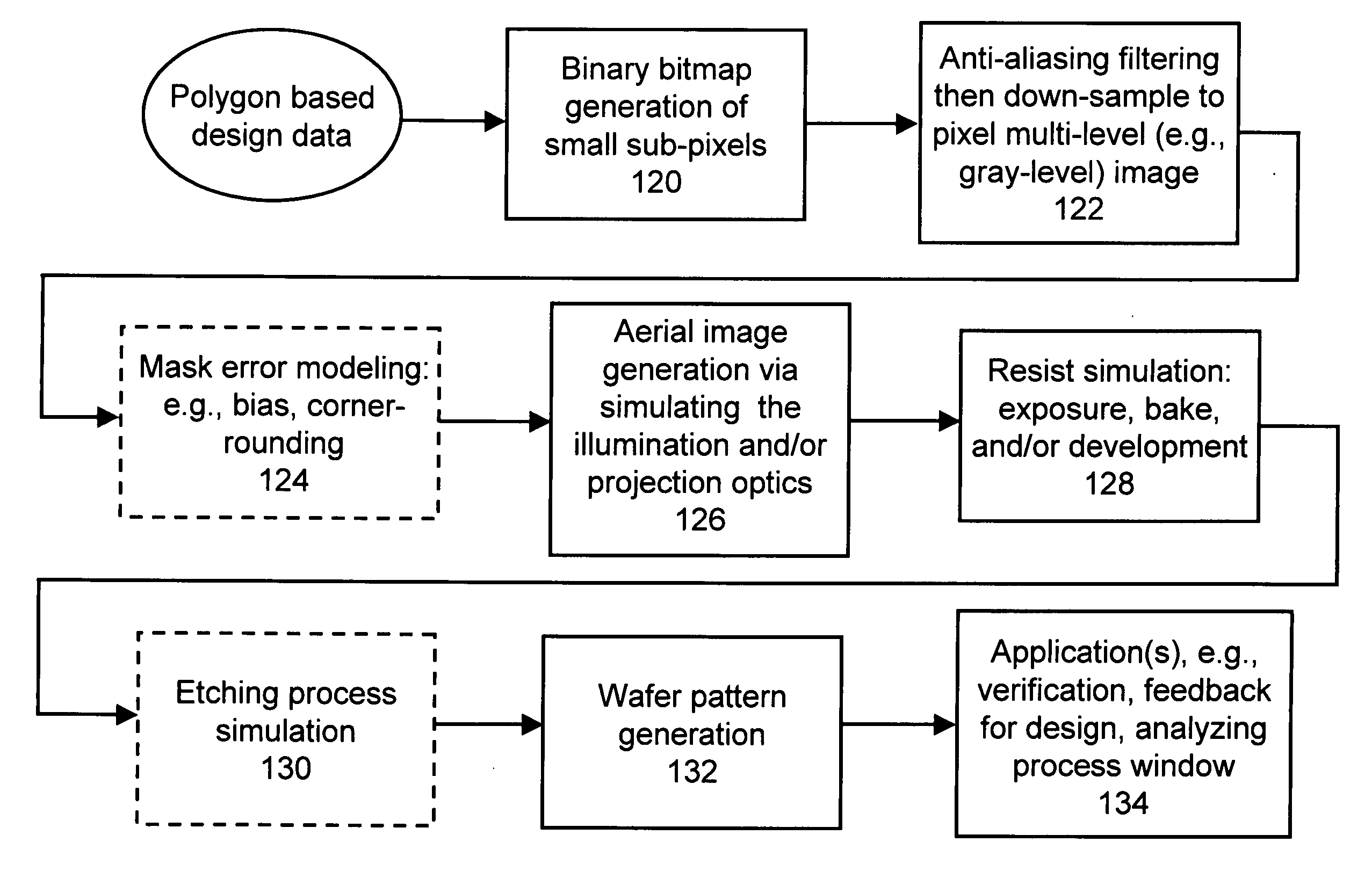
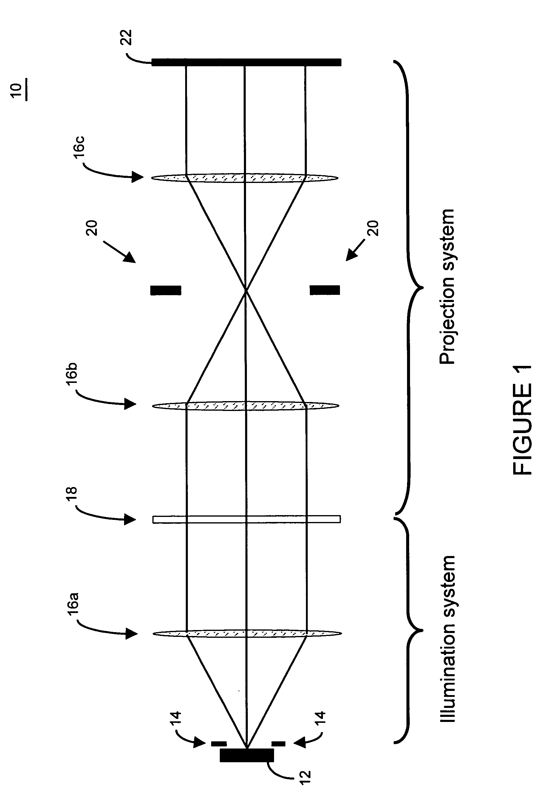
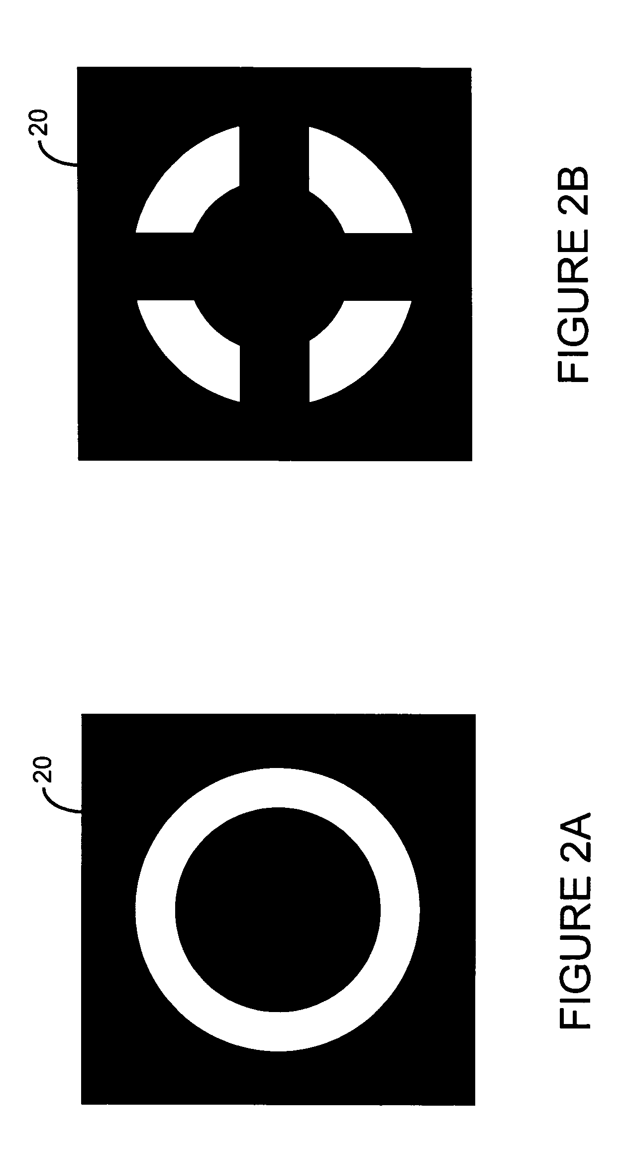
[0041] There are many inventions described and illustrated herein. In one aspect, the present invention is directed to a technique of, and system for simulating, verifying, inspecting, characterizing, determining and / or evaluating the lithographic designs, techniques and / or systems, and / or individual functions performed thereby or components used therein. In one embodiment, the present invention is a system and method that accelerates lithography simulation, inspection, characterization and / or evaluation of the optical characteristics and / or properties, as well as the effects and / or interactions of lithographic systems and processing techniques. In this regard, in one embodiment, the present invention employs a lithography simulation system architecture, including application-specific hardware accelerators, and a processing technique to accelerate and facilitate verification, characterization and / or inspection of a mask design, for example, RET design, including detailed simulation ...


PUM

PropertyMeasurementUnit
thicknessaaaaaaaaaa
thicknessaaaaaaaaaa
sizeaaaaaaaaaa

Abstract

There are many inventions described and illustrated herein. In one aspect, the present invention is directed to a technique of, and system for simulating, verifying, inspecting, characterizing, determining and/or evaluating the lithographic designs, techniques and/or systems, and/or individual functions performed thereby or components used therein. In one embodiment, the present invention is a system and method that accelerates lithography simulation, inspection, characterization and/or evaluation of the optical characteristics and/or properties, as well as the effects and/or interactions of lithographic systems and processing techniques. In this regard, in one embodiment, the present invention employs a lithography simulation system architecture, including application-specific hardware accelerators, and a processing technique to accelerate and facilitate verification, characterization and/or inspection of a mask design, for example, RET design, including detailed simulation and characterization of the entire lithography process to verify that the design achieves and/or provides the desired results on final wafer pattern. The system includes: (1) general purpose-type computing device(s) to perform the case-based logic having branches and inter-dependency in the data handling and (2) accelerator subsystems to perform a majority of the computation intensive tasks.

Description

CROSS-REFERENCE TO RELATED APPLICATIONS [0001] This application claims priority to: U.S. Provisional Application Ser. No. 60 / 509,600, entitled “System and Method of Fast Lithography Simulation”, filed Oct. 7, 2003 (hereinafter “the Provisional Application”). The contents of the Provisional Application are incorporated by reference herein in their entirety.BACKGROUND OF THE INVENTION [0002] This invention relates to systems and techniques that are used to measure, inspect, characterize, simulate and / or evaluate the performance of lithographic systems and techniques; and more particularly, in one aspect, to measure, inspect, characterize, simulate and / or evaluate the optical characteristics and effects of lithographic systems and processing techniques (for example, systems and techniques implemented in the semiconductor fabrication / processing environments). [0003] Briefly, in the semiconductor industry, microlithography (or simply lithography) is the process of printing the circuit pa...

Claims


Application Information

Patent Timeline
Patent Type & Authority Applications(United States)
IPC IPC(8): G03B27/54G03FG03F1/88G03F7/20G06F17/50G06K9/00G06T7/00G16Z99/00
CPCG03F7/705G03F7/70666G06T7/0004G06T2207/30148G03F7/004G06F2217/14G06F17/5081G06F19/00G21K5/00G06F17/5009G06F2217/12G03F1/00G16Z99/00G06F30/20G06F30/398G06F30/333G06F2119/18
Inventor YE, JUNLU, YEN-WENCAO, YACHEN, LUOQICHEN, XUN
Owner ASML NETHERLANDS BV
Why Eureka
Try Eureka