
System and architecture that supports a multi-function semiconductor device between networks and portable wireless communications products

a multi-functional, wireless communication technology, applied in the field of wireless communication, can solve the problems of inability to take advantage of the features and benefits of the others, deficient design, and inability to integrate the capabilities of the three identified components

Inactive Publication Date: 2007-07-03
PRIDDY DENNIS G
View PDF25 Cites 209 Cited by
  • Summary
  • Abstract
  • Description
  • Claims
  • Application Information

AI Technical Summary

Benefits of technology

[0006]It is, therefore, an object of the present invention to overcome the above deficiencies of the prior art and provide users of wireless telecommunications technology an enhanced utility and functionality without diminishing or altering the original capabilities of the host portable two-way communication device.
[0007]Broadly, the present invention is directed to a self-contained integrated imaging module, which is designed to be incorporated into any number of portable host products and which enables users of these products to “see,”“speak,”“show” images, and securely exchange personal or business information with other people and computers. Suitable host products include, but are not limited to, cellular / satellite telephones, wireless empowered Personal Digital Assistants (PDA), portable computers, portable automatic identification terminals, and the like. Miniaturized two-way portable communication devices are preferred. The integrated imaging module preferably includes, among other things, a fully integrated semiconductor device, such as a Complementary Metal-Oxide Semiconductor (CMOS), which enhances host product productivity and capability by allowing users to execute remotely virtually any function. By use of such an integrated imaging module, one can convert an instant personal objective into a machine executable action at a remote location, which may be physically distant or proximate to the user at the time of execution.
[0012]4. secure storage of personal information such as credit / debit card numbers;
[0017]Advantageously, the integrated imaging module of the present invention adds such features, functionalities, and capabilities without diminishing the available memory, computing performance, or previously existing functionality of the host product.
[0021]Another implementation is to provide a secure memory mode of operation. In this, the module contains personal identification data including, for example, credit card / debit card account information, bank account, driver's license number, social security number and the like for executing securely financial transactions. In this regard, the module enhanced product allows the user to execute a secure purchase of non-electronic commerce goods and services.

Problems solved by technology

This design is deficient in that the capabilities of the three identified components are not functionally integrated and each is unable to take advantage of the features and benefits of the others.
The design is effective in determining signal strength and assuring successful transmission of an image, but deficient in that the device does not provide the capabilities of automatic identification, voice communication, or other interactive business functions.
However, the Morris patent is directed to the transmission of video images and does not provide users with a range of complementary functionality.
These terminals are deficient in that they are dedicated to the art of automatic identification and do not provide for the cumulative capability of automatic identification, two-way voice communication, transmission of instantly captured digital images, and the conduct of electronic commerce and personal finance activities, and the advantages appurtenant to such a combination.
Unfortunately, this technique also limits the number of applications, and the size of the applications, to only those that can reside fully within the capacity of the removable memory card.
This system is deficient in that the remote data acquisition instrument acts as a single purpose slave device unable to perform multiple applications or serve as a means of independently activating functions resident on the remote host computer system.

Method used


Image

  • System and architecture that supports a multi-function semiconductor device between networks and portable wireless communications products
  • System and architecture that supports a multi-function semiconductor device between networks and portable wireless communications products
  • System and architecture that supports a multi-function semiconductor device between networks and portable wireless communications products

Examples


Embodiment Construction

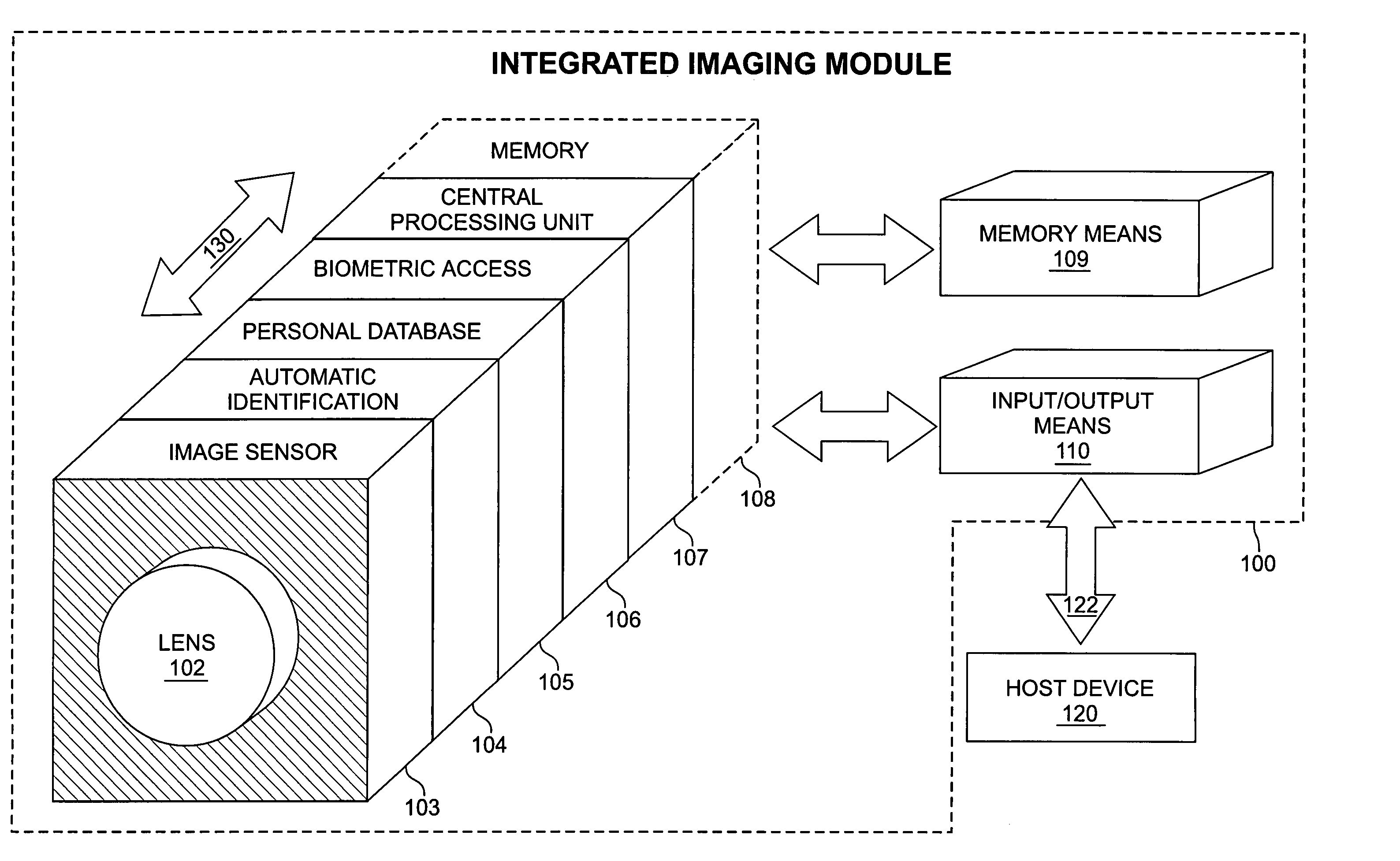
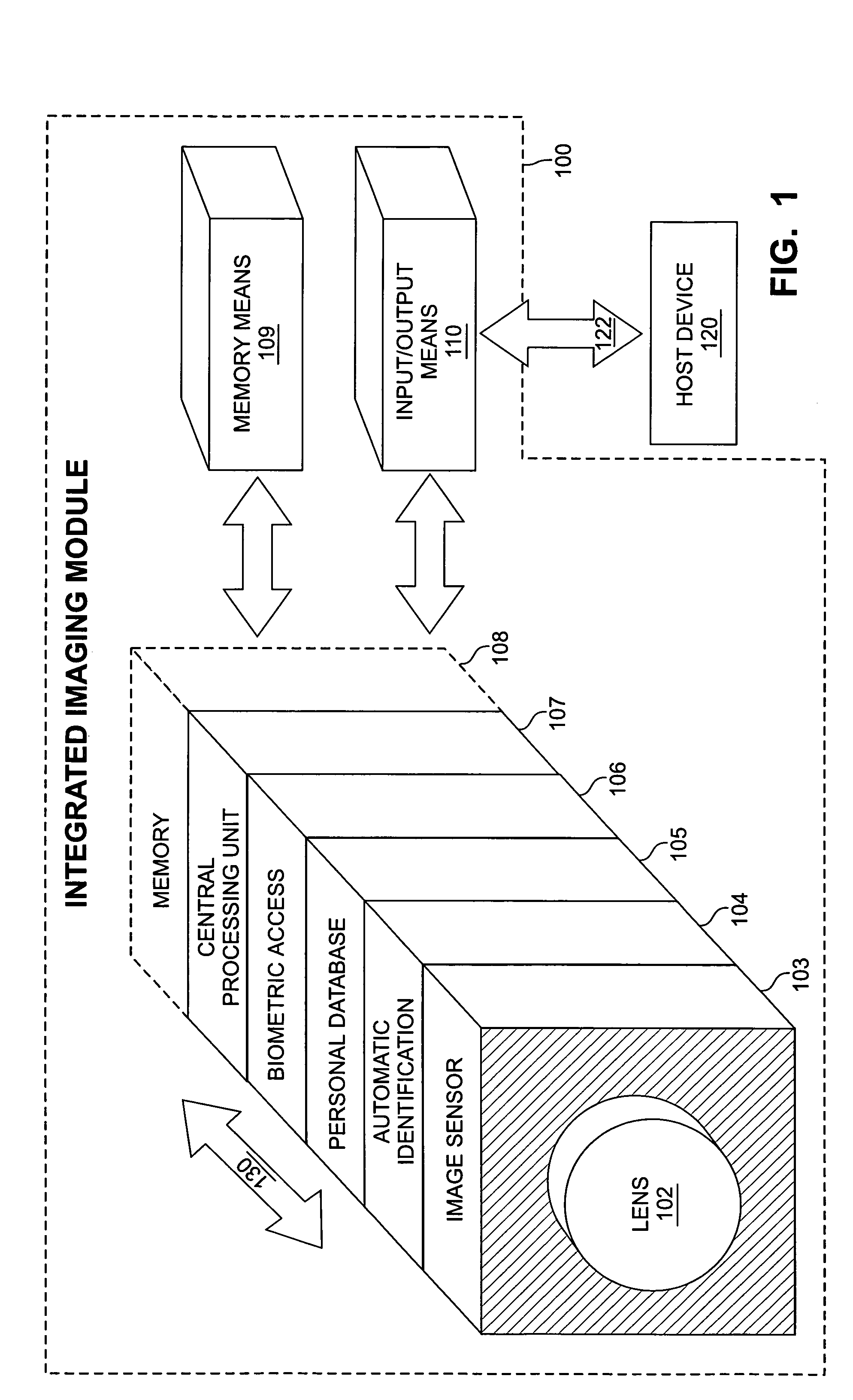
[0034]With reference to FIG. 1, the integrated imaging module 100 of the present invention, is fully self-contained and requires a host portable communications device 120 to supply only an interface 122 and power (not shown). The interface 122 and power can be conveyed to the integrated imaging module 100 either via an internal bus connection to a host device controller board (not shown) or via an external RS232 port of the host (not shown). Module 100 includes a lens assembly 102, which may be comprised of either a single fixed lens, or multiple fixed, extendable, or moveable lens elements. Lens assembly 102 is preferably placed forward of a multi-layered semiconductor device 130. The semiconductor device 130, preferably constructed as a Complementary Metal-Oxide Semiconductor (CMOS) integrated component, has an image sensor layer 103, an automatic identification layer 104, a personal database layer 105, a biometric access layer 106, a central procession unit layer 107, and optiona...


PUM


Abstract

A system and architecture that supports an integrated imaging module for use between networks and portable communications products. The integrated imaging module contains a lens, memory, an input / output device, and a multi-function semiconductor device, such as a Complementary Metal-Oxide Semiconductor (CMOS). Within the design of the multi-function semiconductor device are the functions of still and full-motion digital imaging, image processing, automatic identification, a secure personal database, biometric attribute identification for access control, personal finance information, wireless communication protocols, general purpose processing, and memory. The module may be incorporated into any portable wireless communication product and used to capture text and image data for incorporation into a wireless transmission to a remote device.

Description

FIELD OF THE INVENTION[0001]The present invention is directed to wireless communications, and more particularly to image capture by portable wireless communications products and wireless transmission of data related to the image to a remote location.BACKGROUND OF THE INVENTION[0002]Ornamental designs that incorporate digital cameras with cellular telephones and a portable computer into a single housing are known in the art. One example of such a design is shown in U.S. Pat. Des. 405,457 issued Feb. 9, 1999, to Kawashima. A cellular telephone is illustrated essentially affixed to the side of a digital camcorder with each unit interfaced to a central processor, yet for all purposes, each component operates independently of the other. This design is deficient in that the capabilities of the three identified components are not functionally integrated and each is unable to take advantage of the features and benefits of the others. Another example is found in U.S. Pat. No. 5,917,542 issue...

Claims


Application Information

Patent Timeline
Patent Type & Authority Patents(United States)
IPC IPC(8): H04N5/225H04L9/00H04N7/14H04N21/414H04N21/4223H04N21/4415
CPCG06K9/00885H04N7/142H04N21/41407H04N21/4223H04N21/4415H04N2007/145G06V40/10
Inventor PRIDDY, DENNIS G.
Owner PRIDDY DENNIS G
Learn More