

Structure of a micro electro mechanical system and the manufacturing method thereof
- Summary
- Abstract
- Description
- Claims
- Application Information
AI Technical Summary
Benefits of technology
Problems solved by technology
Method used
Image

Examples
first embodiment
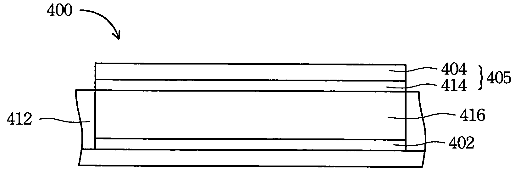
[0032] The
[0033]FIG. 4A to FIG. 4C illustrates a method for manufacturing an optical interference display cell structure in accordance with an embodiment of the present invention. Please referring to FIG. 4A, a first electrode 402 and a sacrificial layer 406 are formed on a transparent substrate 401 in sequence. The material of the sacrificial layer 406 can be transparent material, such as dielectric material, or opaque material, such as metal material. The opening 408, suitable for forming a supporter therein, is formed in the first electrode 402 and the sacrificial layer 406 by a photolithography process.
[0034] Then, a material layer 410 is formed on the sacrificial layer 406 to fill up the opening 408. The material layer 410 is suitable for forming the supporter, and the material layer 410 is generally made of photosensitive materials such as photoresists, or non-photosensitive polymer materials such as polyester, polyamide etc. If non-photosensitive materials are used for formi...
second embodiment
[0039] The
[0040]FIG. 5A to FIG. 5D illustrate a method for manufacturing an optical interference display cell structure in accordance with an alternative embodiment of the present invention. Please referring to FIG. 5A, a first electrode 502 and a sacrificial layer 506 are formed on a transparent substrate 501 in sequence. The material of the sacrificial layer 506 can be transparent material, such as dielectric material, or opaque material, such as metal material. The opening 508, suitable for forming a supporter therein, is formed in the first electrode 502 and the sacrificial layer 506 by a photolithography process.
[0041] Then, a material layer 510 is formed on the sacrificial layer 506 to fill up the opening 508. The material layer 510 is suitable for forming the supporter, and the material layer is generally made of photosensitive materials such as photoresists, or non-photosensitive polymer materials such as polyester, polyamide etc. If non-photosensitive materials are used fo...
third embodiment
[0047] The
[0048]FIG. 6A to FIG. 6D illustrate a method for manufacturing an optical interference display cell structure in accordance with another embodiment of the present invention. Please referring to FIG. 6A, a first electrode 602 and a sacrificial layer 606 are formed on a transparent substrate 601 in sequence. The material of the sacrificial layer 606 can be transparent material, such as dielectric material, or opaque material, such as metal material. The opening 608, suitable for forming a supporter therein, is formed in the first electrode 602 and the sacrificial layer 606 by a photolithography process.
[0049] Then, a material layer 610 is formed on the sacrificial layer 606 to fill up the opening 608. The material layer 610 is suitable for forming the supporter, and the material layer is generally made of photosensitive materials such as photoresists, or non-photosensitive polymer materials such as polyester, polyamide etc. If non-photosensitive materials are used for formi...
PUM
| Property | Measurement | Unit |
|---|---|---|
| Thickness | aaaaa | aaaaa |
| Dielectric polarization enthalpy | aaaaa | aaaaa |
| Structure | aaaaa | aaaaa |
Abstract
Description
Claims
Application Information