Etching method for forming a square cornered polysilicon wordline electrode

a polysilicon and wordline electrode technology, applied in the direction of semiconductor devices, electrical equipment, basic electric elements, etc., can solve the problems of affecting the reliability of write and erase operations, affecting the stability of control gates, and achieving acceptable etching profiles of polysilicon structures

Inactive Publication Date: 2005-04-14
TAIWAN SEMICON MFG CO LTD
View PDF9 Cites 6 Cited by
  • Summary
  • Abstract
  • Description
  • Claims
  • Application Information

AI Technical Summary

Benefits of technology

[0007] To achieve the foregoing and other objects, and in accordance with the purposes of the present invention as embodied and broadly described herein, the present invention provides a split gate FET wordline electrode structure and method for forming the same including a split gate FET wordline electrode structure and method for forming the same including an improved polysilicon etching process.

Problems solved by technology

For example, the polysilicon spacer (electrode) profile can affect the series resistance and hence the electrical stability of the control gate, for example, including altering hot electron injection processes or Fowler-Nordheim tunneling processes which adversely affect the stability of the control gate thereby adversely affecting the reliability of write and erase operations, both processes essential to the reliable operation of flash memory devices.
As design rules have decreased to below about 0.25 micron technology, achieving acceptable etching profiles of the polysilicon structures has become increasingly difficult due to several hard to control RIE etching phenomena including polymeric residue formation and micro-trenching as a result of secondary plasma ion bombardment.
In addition, problems are presented in RIE etching processes where different doping levels of polysilicon are present causing variable etching rates.
One particular problem in polysilicon RIE etching processes, for example in the formation of a self aligned polysilicon structure, is preferential etching and accumulation of polymeric RIE etching residues at an upper portion of the polysilicon structure to produce a fence or raised portion at outer edges of the upper portion of the polysilicon structure.
For example, during prior art RIE etching processes to form self aligned polysilicon wordline electrodes, the formation of fences which are composed of a hardmask and polysilicon layer at an outer edge of the upper portion of the polysilicon structure has been a recurring problem which undesirably alters the etching profile of the polysilicon structure to cause undesired variations in polysilicon electrical resistances and presents the potential for causing electrical shorting to subsequently formed overlying wiring, for example, bit lines.

Method used


Image

  • Etching method for forming a square cornered polysilicon wordline electrode
  • Etching method for forming a square cornered polysilicon wordline electrode
  • Etching method for forming a square cornered polysilicon wordline electrode

Examples


Embodiment Construction

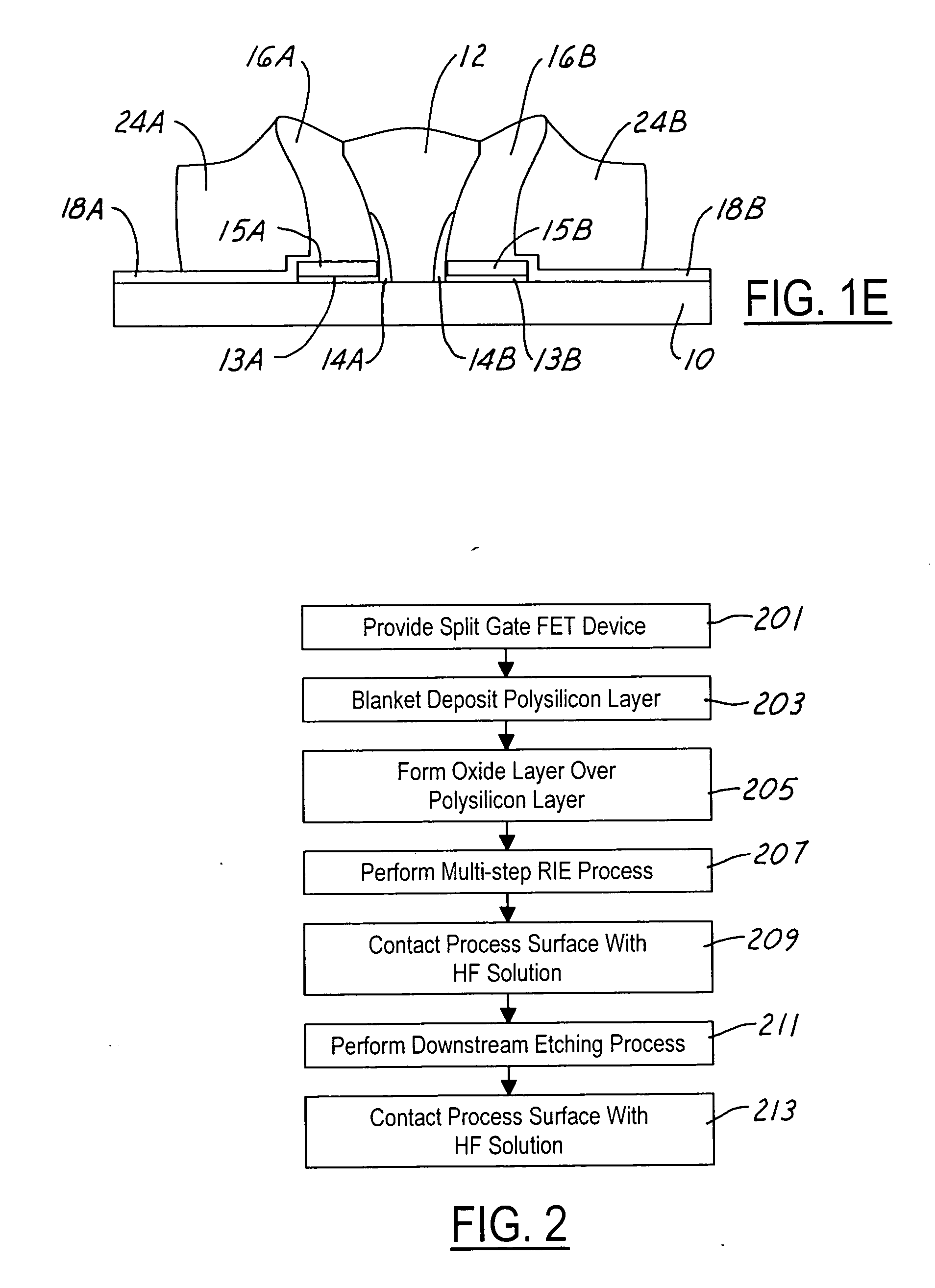
[0012] Although the method of the present invention is explained with reference to an exemplary embodiment including the formation of square-shouldered (box-shaped) self aligned wordline electrodes in a split gate configuration for use in an EEPROM (flash memory) device, it will be appreciated that the method of the present invention may be advantageously used in the formation of any self-aligned polysilicon structure where the polysilicon structure is advantageously etched to provide a square-shouldered profile while avoiding preferential RIE etching in an upper portion of the polysilicon structure.

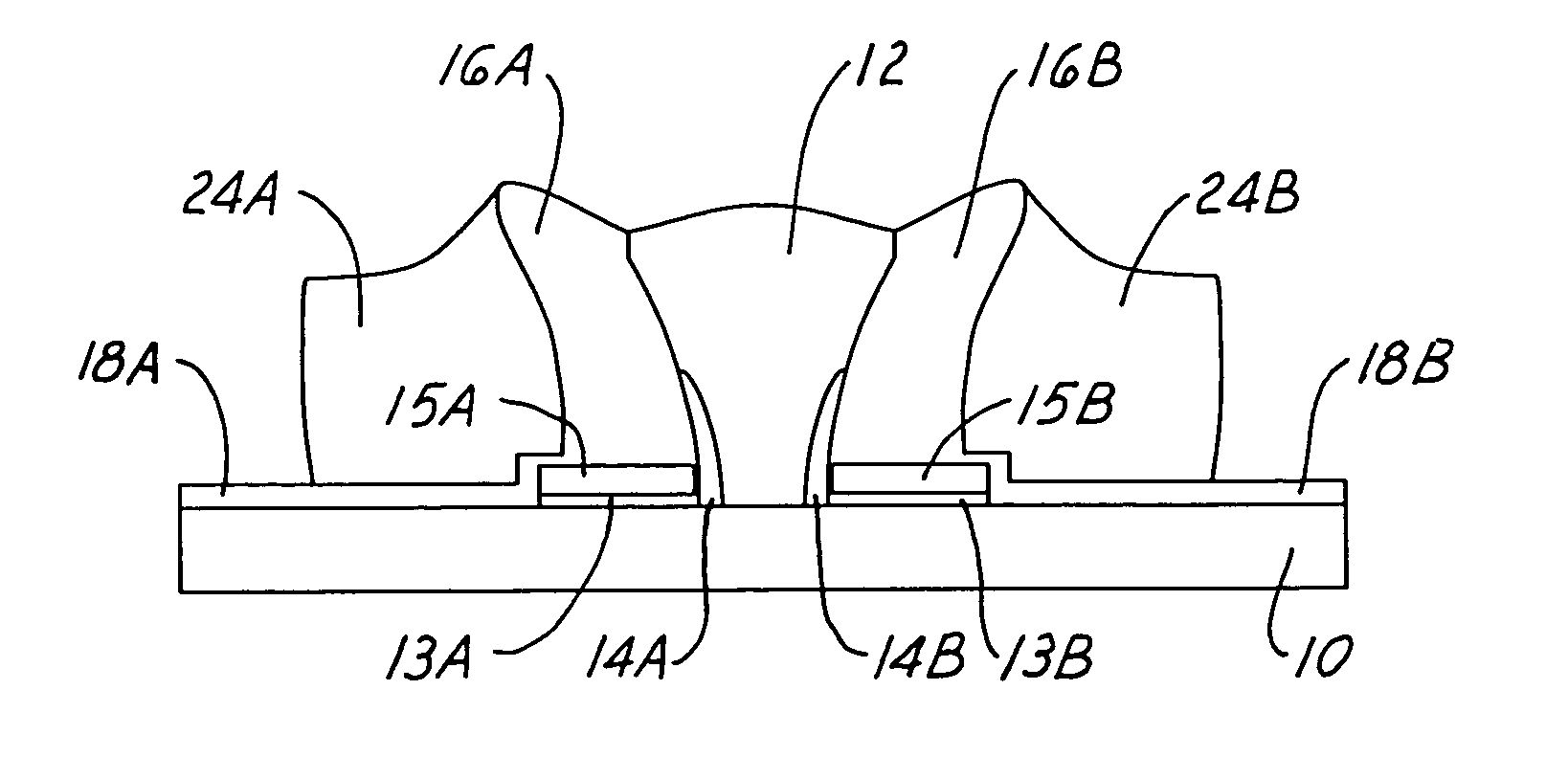
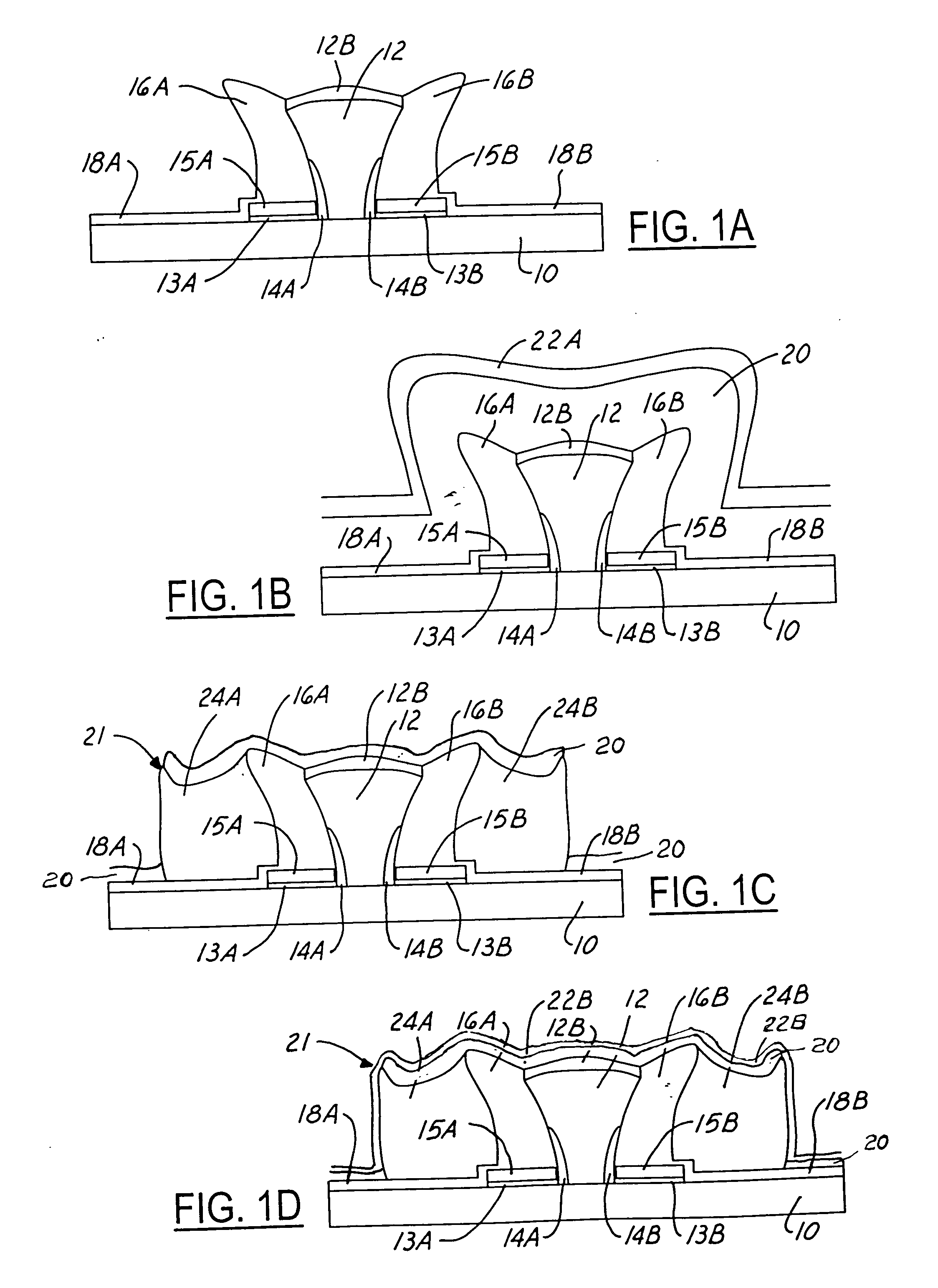
[0013] For example referring to FIGS. 1A to 1E, are shown cross sectional schematic views of an exemplary portion of a memory cell including a split gate FET structure at stages in manufacture for use in a flash memory device.

[0014] Shown in FIG. 1A is source polysilicon gate structures 12 formed over doped silicon substrate (e.g., wafer) 10 including doped source regions (not shown) f...


PUM


Abstract

A split gate FET wordline electrode structure and method for forming the same including an improved polysilicon etching process including providing a semiconductor wafer process surface comprising first exposed polysilicon portions and adjacent oxide portions; forming a first oxide layer on the exposed polysilicon portions; blanket depositing a polysilicon layer on the first exposed polysilicon portions and adjacent oxide portions; forming a hardmask layer on the polysilicon layer; carrying out a multi-step reactive ion etching (RIE) process to etch through the hardmask layer and etch through a thickness portion of the polysilicon layer to form second polysilicon portions adjacent the oxide portions having upward protruding outer polysilicon fence portions; contacting the semiconductor wafer process surface with an aqueous HF solution; and, carrying out a downstream plasma etching process to remove polysilicon fence portions.

Description

FIELD OF THE INVENTION [0001] This invention generally relates to processing method for forming semiconductor device structures, and more particularly to a method for forming self-aligned polysilicon wordline electrodes for use with a split gate FET flash memory device. BACKGROUND OF THE INVENTION [0002] In the flash EEPROM (Electrically Erasable Programmable Read Only Memories) including split gate FET devices, for example, including polysilicon source and wordline electrodes, the level of the voltage required to be applied to the control gate in a split gate field effect transistor (TET) flash memory device structure is critical and is affected by the profile of the polysilicon electrode, also referred to as a wordline spacer which functions as the control gate in a split gate flash memory configuration. For example, the polysilicon spacer (electrode) profile can affect the series resistance and hence the electrical stability of the control gate, for example, including altering ho...

Claims


Application Information

Patent Timeline
Patent Type & Authority Applications(United States)
IPC IPC(8): H01L21/311H01L21/3213H01L21/336H01L21/8247H01L27/115
CPCH01L21/31116H01L21/32137H01L27/11521H01L21/32139H01L27/115H01L21/32138H10B69/00H10B41/30
Inventor OUYANG, HSIULO, CHI-HSINHUANG, CHEN-MINGHSIEH, CHIA-TATSAI, CHIA-SHIUNG
Owner TAIWAN SEMICON MFG CO LTD
Why Eureka
Try Eureka