Method of manufacturing a trench transistor having a heavy body region

a manufacturing method and transistor technology, applied in the field of field effect transistors, can solve the problems of high threshold, high on-state resistance, and potential non-functional transistors, and achieve the effects of high cell density, easy scaling, and good uniformity

Inactive Publication Date: 2005-04-14
SEMICON COMPONENTS IND LLC
View PDF90 Cites 35 Cited by
  • Summary
  • Abstract
  • Description
  • Claims
  • Application Information

AI Technical Summary

Benefits of technology

[0007] The present invention provides field effect transistors that have an open cell layout that provides good uniformity and high cell density and that is readily scalable. Preferred trenched DMOS transistors exhibit low Rdson, low parasitic capacitance, excellent reliability, resistance to avalanche breakdown degradation, and ruggedness. Preferred devices also include a field termination that enhances resistance to avalanche breakdown. The invention also features a method of making trench DMOS transistors.

Problems solved by technology

If the recess is deeper than the source junctions the source may miss the gate, resulting in high on-state resistance, high threshold, and potentially a non-functional transistor.
Punchthrough occurs when, upon application of a high drain to source voltage, depletion into the body region extends to the source region, forming an undesirable conductive path through the body region when the transistor should be off.

Method used


Image

  • Method of manufacturing a trench transistor having a heavy body region
  • Method of manufacturing a trench transistor having a heavy body region
  • Method of manufacturing a trench transistor having a heavy body region

Examples


Embodiment Construction

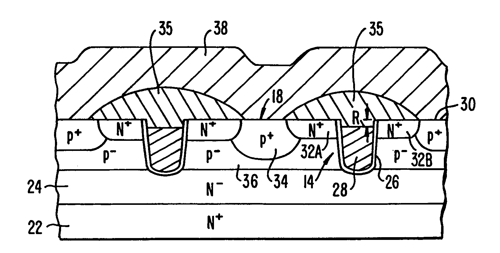
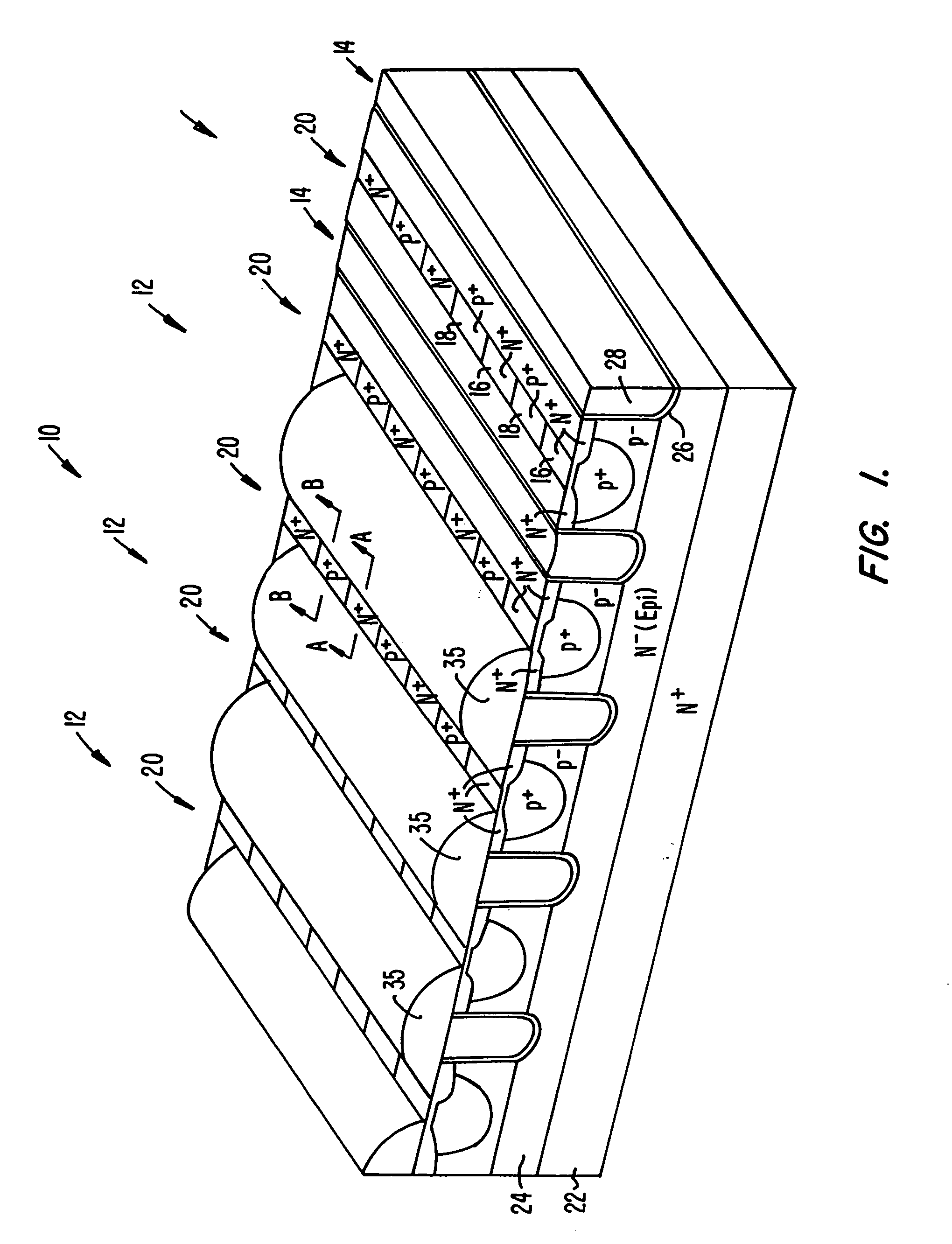
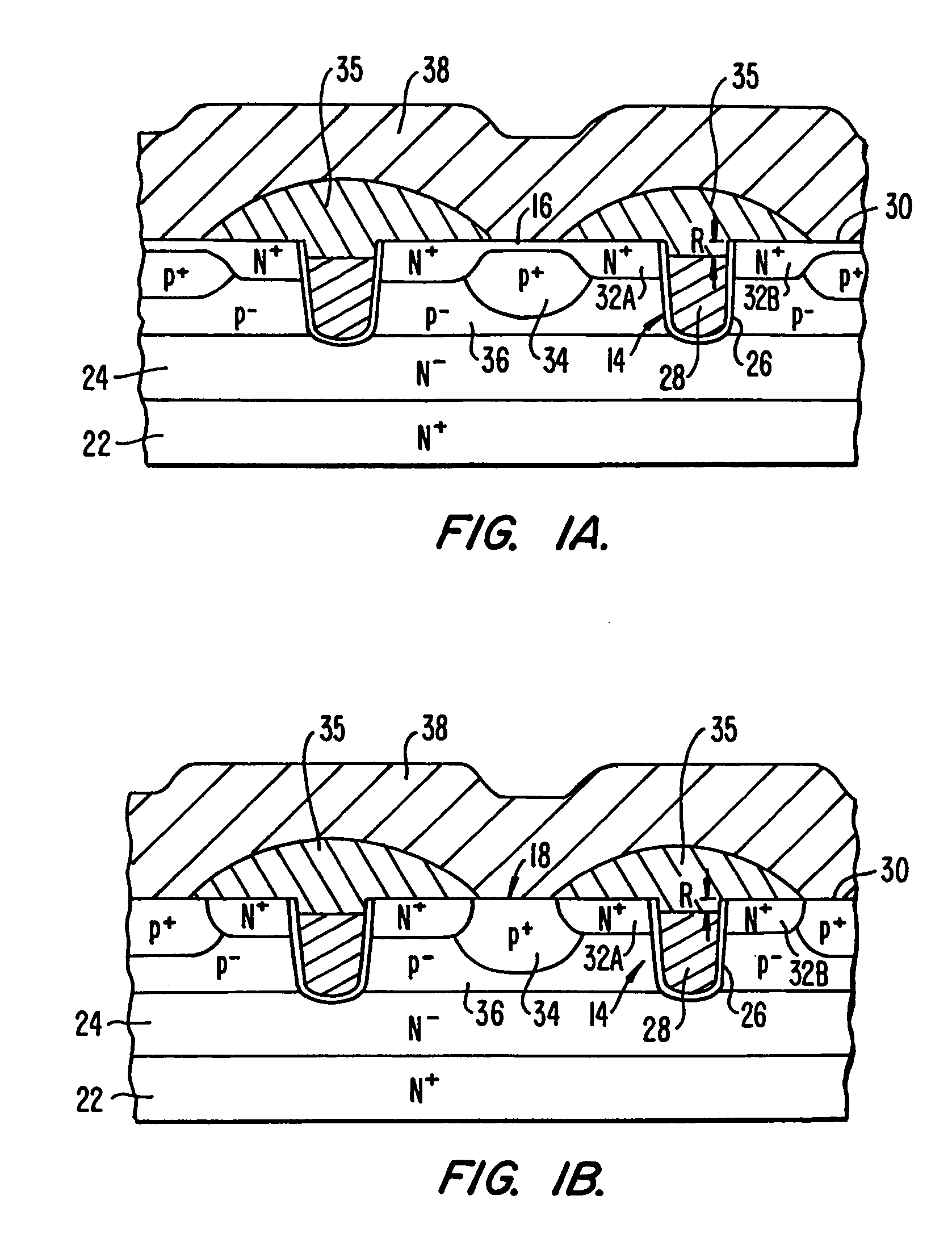
[0025] A cell array 10, including a plurality of rows 12 of trenched DMOS transistors, is shown in FIG. 1. Cell array 10 has an open cell configuration, i.e., trenches 14 run in only one direction, rather than forming a grid. Individual cells are formed by alternating n+ source contacts 16 and p+ contacts 18 in rows 20 that run parallel to and between trenches 14. The configuration of the regions of each row that have an n+ source contact are shown in cross-section in FIG. 1a, while the regions that have a p+ contact are shown in FIG. 1b.

[0026] As shown in FIGS. 1a and 1b, each trenched DMOS transistor includes a doped n+ substrate (drain) layer 22, a more lightly doped n− epitaxial layer 24, and a gate electrode 28. Gate electrode 28 comprises a conductive polysilicon that fills a trench 14. A gate oxide 26 coats the walls of the trench and underlies the polysilicon. The top surface of the polysilicon is recessed from the surface 30 of the semiconductor substrate by a distance R (...


PUM


Abstract

A trenched field effect transistor is provided that includes (a) a semiconductor substrate, (b) a trench extending a predetermined depth into the semiconductor substrate, (c) a pair of doped source junctions, positioned on opposite sides of the trench, (d) a doped heavy body positioned adjacent each source junction on the opposite side of the source junction from the trench, the deepest portion of the heavy body extending less deeply into said semiconductor substrate than the predetermined depth of the trench, and (e) a doped well surrounding the heavy body beneath the heavy body.

Description

[0001] This application is a continuation of and claims the benefit of U.S. application Ser. No. 10 / 347,254, filed Jan. 17, 2003, which is a continuation of U.S. application Ser. No. 09 / 854,102 filed May 9, 2001, which is a divisional of U.S. application Ser. No. 08 / 970,221 filed Nov. 14, 1997.BACKGROUND OF THE INVENTION [0002] The present invention relates to field effect transistors, in particular trench DMOS transistors, and methods of their manufacture. [0003] Power field effect transistors, e.g., MOSFETs (metal oxide semiconductor field effect transistors), are well known in the semiconductor industry. One type of MOSFET is a DMOS (double diffused metal oxide semiconductor) transistor. DMOS transistors typically include a substrate on which an epitaxial layer is grown, a doped source junction, a doped heavy body, a doped well of the same (p or n) doping as the heavy body, and a gate electrode. In trenched DMOS transistors the gate electrode is a vertical trench. The heavy body ...

Claims


Application Information

Patent Timeline
Patent Type & Authority Applications(United States)
IPC IPC(8): H01L21/336H01L29/06H01L29/10H01L29/78
CPCH01L29/0619H01L29/0696H01L29/0869H01L29/1095H01L29/7813H01L29/4236H01L29/66734H01L29/7811H01L29/407H01L29/78
Inventor MO, BRIAN SZE-KICHAU, DUCSAPP, STEVENBENCUYA, IZAKPROBST, DEAN E.
Owner SEMICON COMPONENTS IND LLC
Why Eureka
Try Eureka