Method for cleaning elements in vacuum chamber and apparatus for processing substrates

a vacuum chamber and element technology, applied in the direction of cleaning using liquids, chemistry apparatus and processes, electric discharge tubes, etc., can solve the problems of reducing the production yield of the finally produced semiconductor devices, reducing the efficiency of removing particles with a brush scrubber or a wiper blade under reduced pressure, and causing the effect of causing

Active Publication Date: 2005-04-21
TOKYO ELECTRON LTD
View PDF13 Cites 24 Cited by
  • Summary
  • Abstract
  • Description
  • Claims
  • Application Information

AI Technical Summary

Benefits of technology

[0009] In view of the above problems, it is an object of the present invention to provide an element cleaning method that removes particles from the surface of an element in a vacuum chamber by effectively causing the particles to scatter, a substrate processing apparatus that is equipped with means for implementing the cleaning method, a scattering particle detecting apparatus that monitors the cleaning, a method for evaluating cleanness, and a method for detecting the end point of the cleaning.
[0011] In a second aspect of the invention, particles sticking to the element are electrically charged, and a voltage of the same polarity as the charge of the charged particles is applied to the element, thereby causing the particles sticking to the element to scatter.

Problems solved by technology

In particular, if the stage installed in a vacuum chamber is contaminated with particles, the particles may stick to the underside of the substrate mounted thereon, and the contamination may spread in subsequent steps, eventually rendering the final products defective.
At this time, if the particles P are left sticking to the stage 2, they stick to the underside of the substrate during processing, and the contamination spreads in subsequent steps, leading to such problems as a reduced production yield of the finally produced semiconductor devices.
However, since such cleaning means usually requires opening the lid of the chamber and thus exposing the chamber to the atmosphere, the cleaning itself can cause contamination.
Further, using a brush scrubber or a wiper blade under reduced pressure is not effective in removing particles (for examples, particles with particle size of about 10 nm); on the contrary, this runs the risk of generating new particles due to physical friction.
On the other hand, cleaning the stage with a liquid requires a complicated structure for cleaning, and greatly reduces throughput.
Moreover, by simply spraying a gas, it is difficult to thoroughly clean the stage, because the collision cross section between the particle and the gas is very small.

Method used


Image

  • Method for cleaning elements in vacuum chamber and apparatus for processing substrates
  • Method for cleaning elements in vacuum chamber and apparatus for processing substrates
  • Method for cleaning elements in vacuum chamber and apparatus for processing substrates

Examples


embodiment 1

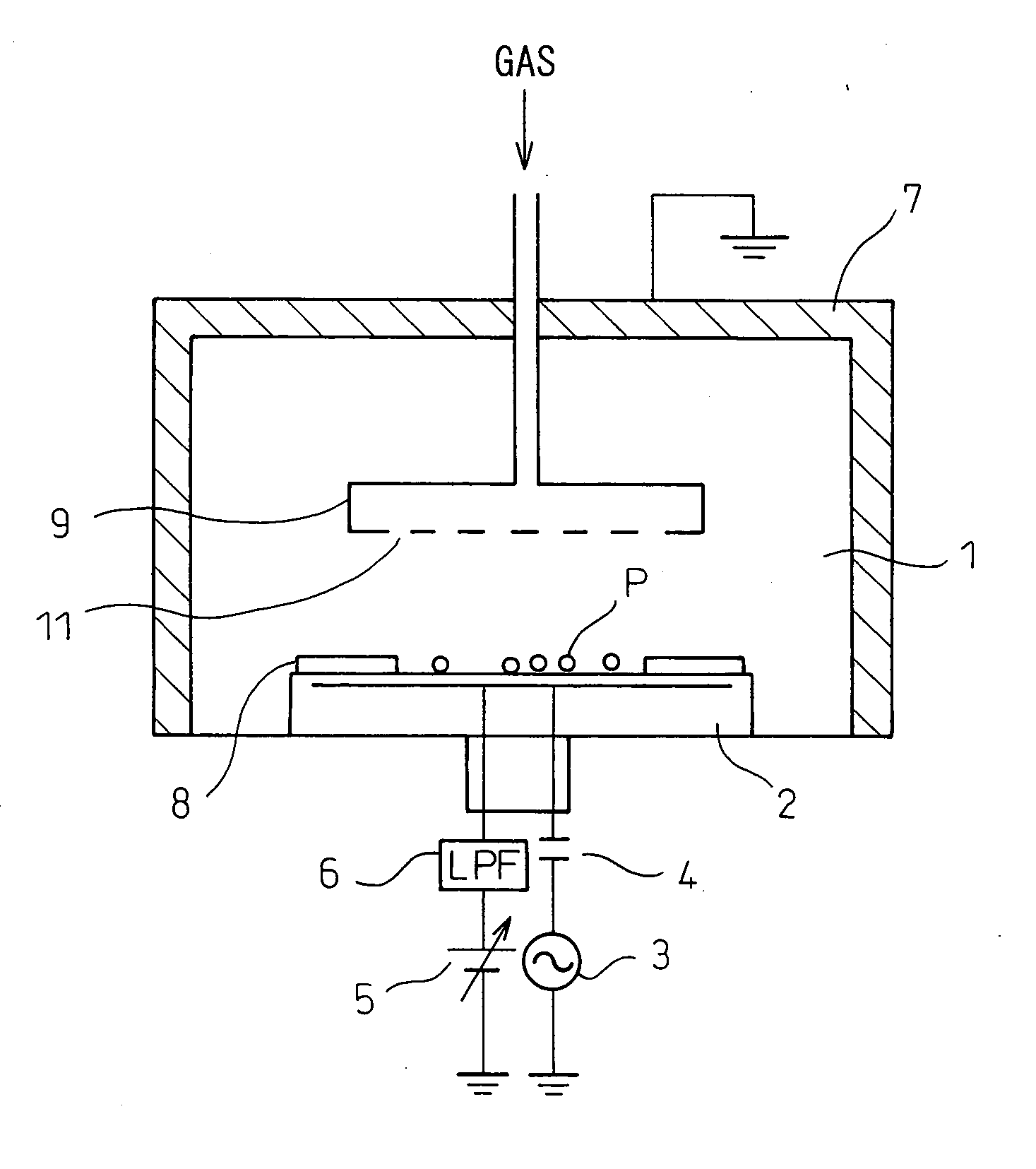
[0055] In this embodiment, in case where there is a large difference between the permittivity of the stage surface and the permittivity of the particles, a predetermined electric field is formed on the surface of the stage in accordance with the second term of Maxwell's stress equation, and the particles are caused to scatter by the resulting repelling force.

[0056] More specifically, before the substrate to be processed is placed on the stage, a positive or negative voltage is applied to the stage by an electrostatic power supply unit such as shown in FIG. 1. An electric field appears at the surface via a dielectric on the surface of the stage. The strength of the electric field at the surface of the stage is considered to depend on the permittivity and thickness of the dielectric on the surface of the stage but, according to an experiment, a voltage approximately equal to the applied voltage appeared, and the strength of the electric field did not suffer attenuation due to the pre...

embodiment 2

[0063] When utilizing the difference between the permittivity of the stage surface and the permittivity of the particles as described in the first embodiment above, the effect can be further enhanced by coating the stage surface with a material having permittivity sufficiently larger than that of the particles expected to stick to the surface. Generally, in an environment where the stage surface is likely to be contaminated by the stick of silicon particles, a greater effect can be obtained if the stage surface is coated with a material having permittivity sufficiently larger than 11.

[0064] Examples of such materials include Bi2O3 (permittivity 18.2), CuO (permittivity 18.1), FeO (permittivity 14.2), KH2PO4 (permittivity 46), KIO3 (permittivity 16.85), PbBr2 (permittivity>30), PbCl2 (permittivity 33.5), PbCO3 (permittivity 18.6), PbI2 (permittivity 20.8), Pb(NO3)2 (permittivity 16.8), PbO (permittivity 25.9), PbSO4 (permittivity 14.3), SrSO4 (permittivity 18.5), TiO2 (permittivity ...

embodiment 3

[0065] In the first embodiment, the forces acting on the particles are exerted throughout the application of the voltage but, as previously shown in FIG. 3, the number of scattered particles greatly increases when the voltage changes (in particular, the instant that the voltage is applied). To utilize this phenomenon, a voltage of rectangular waveform may be applied repetitively to the stage. By so doing, the particles can be efficiently caused to scatter as the voltage is applied and stopped. Since it is the change in voltage that serves to promote the scattering of the particles, the waveform need not be limited to the rectangular waveform, but any other waveform, such as a pulse waveform or a sine waveform, may be used.

[0066] The reason is believed to be that particles easier to scatter are scattered at the first application of the voltage and the particles remaining to be scattered are given another change to scatter when the applied voltage is temporarily removed and the volta...


PUM

PropertyMeasurementUnit
pressureaaaaaaaaaa
pressureaaaaaaaaaa
pressureaaaaaaaaaa

Abstract

To clean an element in a vacuum chamber by causing particles sticking to the element to scatter, the present invention uses a means for applying a voltage to the element and causing the particles to scatter by utilizing Maxwell's stress, a means for electrically charging the particles and causing the particles to scatter by utilizing the Coulomb force, a means for introducing a gas into the vacuum chamber and causing the particles sticking to the element to scatter by causing a gas shock wave to hit the element, a means for heating the element and causing the particles to scatter by utilizing the thermal stress and thermophoretic force, or a means for causing the particles to scatter by applying mechanical vibrations to the element. The thus scattered particles are removed by carrying them in a gas flow in a relatively high pressure atmosphere.

Description

BACKGROUND OF THE INVENTION [0001] 1. Field of the Invention [0002] The present invention relates to a technique for cleaning elements in a vacuum chamber and, more particularly, to a technique for cleaning a stage, or the like, for holding, for example, a substrate to be processed. [0003] 2. Description of the Related Art [0004] In the manufacturing processes of semiconductors or flat panel displays (FPDs) such as liquid crystal displays, a major concern is to prevent substrates, during processing, being contaminated with particles entering from outside the manufacturing equipment or generated within the manufacturing equipment. In particular, if the stage installed in a vacuum chamber is contaminated with particles, the particles may stick to the underside of the substrate mounted thereon, and the contamination may spread in subsequent steps, eventually rendering the final products defective. [0005]FIG. 1 shows a schematic diagram of a conventional plasma etching apparatus. A stag...

Claims


Application Information

Patent Timeline
Patent Type & Authority Applications(United States)
IPC IPC(8): B08B5/02B08B3/12B08B6/00B08B7/00C23F1/00H01L21/00H01L21/30H01L21/304H01L21/683
CPCB08B3/12H01L21/6831H01L21/67028H01J37/32862H01L21/30
Inventor MORIYA, TSUYOSHINAGAIKE, HIROSHINAKAYAMA, HIROYUKI
Owner TOKYO ELECTRON LTD
Why Eureka
Try Eureka