Nitride-based light emitting device and method of manufacturing the same

a light emitting device and nitride technology, applied in semiconductor lasers, semiconductor/solid-state device details, lasers, etc., can solve the problems of low light utilization efficiency, and the limitation of realizing the next-generation light emitting device with large capacity and high brightness. , to achieve the effect of high light transmittance and low specific contact resistivity

Active Publication Date: 2005-04-21
SAMSUNG ELECTRONICS CO LTD +1
View PDF7 Cites 27 Cited by
  • Summary
  • Abstract
  • Description
  • Claims
  • Application Information

AI Technical Summary

Benefits of technology

[0011] The present invention provides a nitride-based light emitting device with a p-type conductive transparent oxide thin film elect

Problems solved by technology

However, since TLEDs using Ni/Au semi-transparent film electrode contains Au that reduce light transmittance, they suffer the limitation of realizing next generation light emitting devices with large capacity and high brightness due to their low light utilization efficiency.
However, the FCLED also suffers from problems such as high resistance due to poor adhesion and oxidation of a reflective layer.
However, while increasing the output power of a light emitting device, an ITO ohmic contact layer fe

Method used


Image

  • Nitride-based light emitting device and method of manufacturing the same
  • Nitride-based light emitting device and method of manufacturing the same
  • Nitride-based light emitting device and method of manufacturing the same

Examples


first embodiment

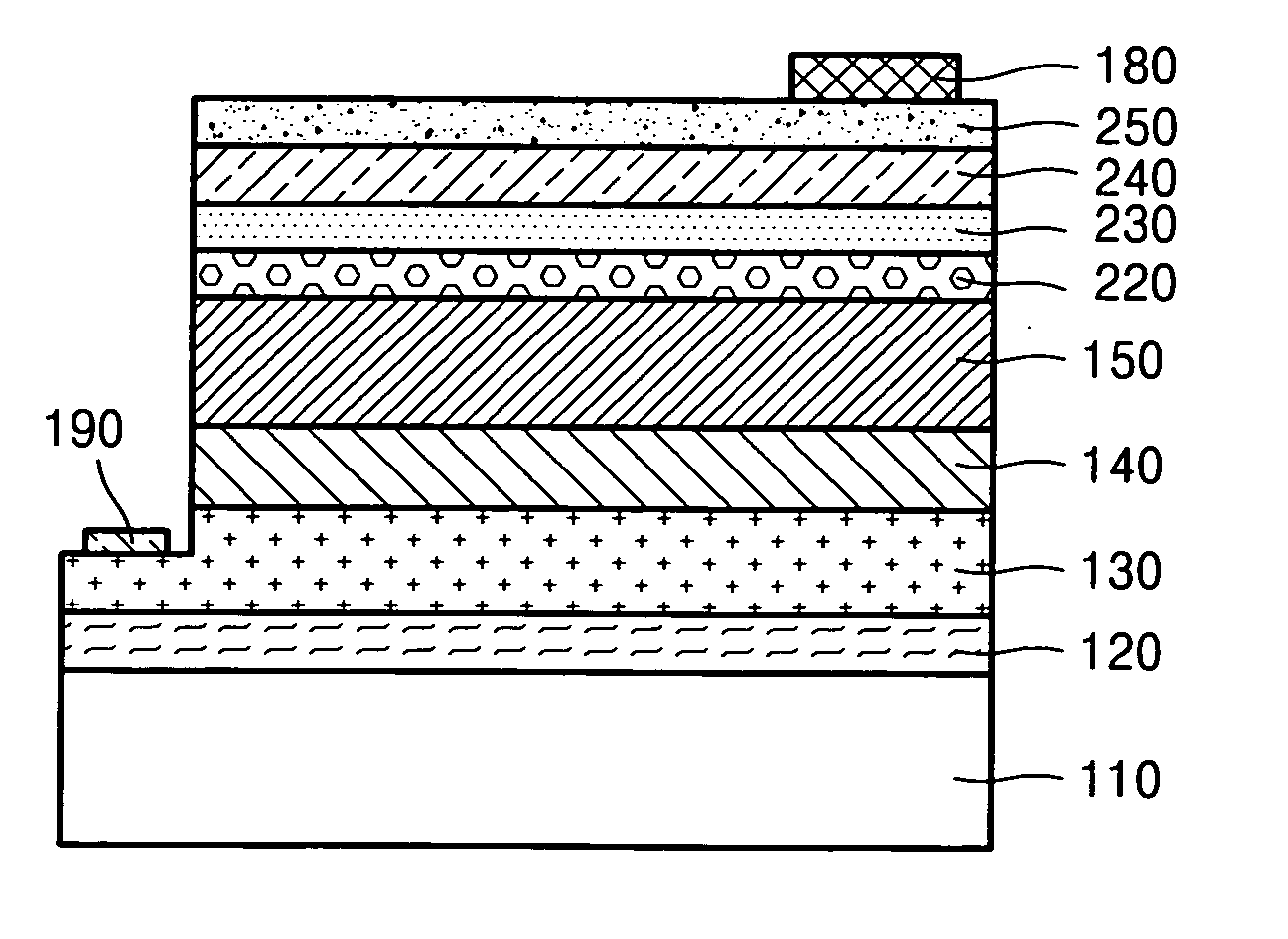
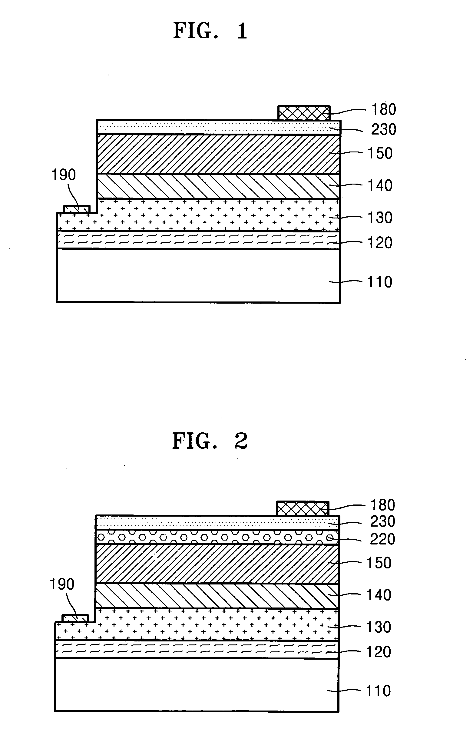
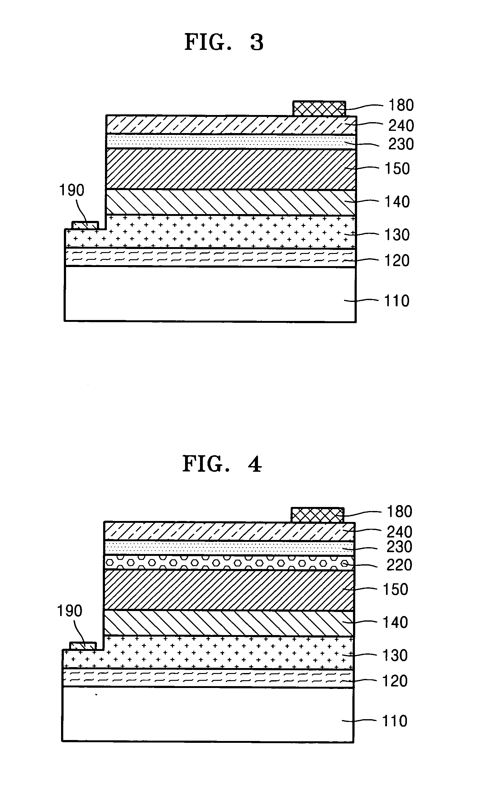
[0032] Referring to FIG. 1, a light emitting device with a p-electrode structure according to the present invention includes a substrate 110, and a buffer layer 120, an n-cladding layer 130, an active layer 140, a p-cladding layer 150 and an ohmic contact layer 230 sequentially formed on the substrate 110. The light emitting device further includes a p-electrode pad 180 and an n-electrode pad 190.

[0033] The substrate 110 may be formed from one of sapphire, silicon carbide (SiC), Si, and GaAs. The buffer layer 120 may not be formed. Each of the layers from the buffer layer 120 up to the p-cladding layer 150 is basically made from a compound selected among III-nitride-based compounds represented by the general formula AlxInyGazN (0≦x≦1, 0≦y≦1, 0≦z≦1, 0≦x+y+z≦1), and the n- and p-cladding layers 130 and 150 contain appropriate dopants in addition to the compounds. The active layer 140 may be formed as a single layer or a multiquantum well (MQW) layer or in other various ways known in t...

second embodiment

[0048]FIG. 2 is a cross-sectional view of a light emitting device with a p-electrode structure according to the present invention. Referring to FIG. 2, the light emitting device includes an insertion layer 220 between an ohmic contact layer 230 and a p-cladding layer 150. That is, the p-electrode structure includes the insertion layer 220 and the ohmic contact layer 230. The insertion layer 220 can be made of a material that helps to form another transparent conductive oxide during annealing after deposition as well as gallide that is a gallium-based compound in order to increase effective carrier (hole) concentration on the surface of the p-cladding layer 150.

[0049] To satisfy the requirements, the insertion layer 220 is made of at least one selected from the group consisting of Ni, NixOy, Au, Pt, Pd, Mg, Cu, CuxOy, Zn, Ag, Sc, Co, CoxOy, Rh, Li, Be, Ca, Ru, Re, Ti, Ta, Na, and La.

[0050] Since the insertion layer 220 helps not only to adjust the carrier concentration in the ohmic ...

third embodiment

[0051]FIG. 3 is a cross-sectional view of a light emitting device with a p-electrode structure according to the present invention. Referring to FIG. 3, the light emitting device includes a reflective layer 240 overlying an ohmic contact layer 230. That is, the p-electrode structure includes the ohmic contact layer 230 and the reflective layer 240. The reflective layer 240 is used for realization of a flip-chip light emitting device and may contain at least one metal selected from the group consisting of Ag, Al, Zn, Mg, Ru, Ti, Rh, Cr, and Pt. The reflective layer 240 may be formed to a thickness of 100 to 2,000 nm.

[0052]FIG. 4 shows an example of a light emitting device including the reflective layer 240 in addition to the light emitting device structure of FIG. 2.


PUM


Abstract

Provided are a nitride-based light emitting device using a p-type conductive transparent thin film electrode layer and a method of manufacturing the same. The nitride-based light emitting device includes a substrate, and an n-cladding layer, an active layer, a p-cladding layer and an ohmic contact layer sequentially formed on the substrate. The ohmic contact layer is made from a p-type conductive transparent oxide thin film. The nitride-based light emitting device and method of manufacturing the same provide excellent I-V characteristics by improving characteristics of an ohmic contact to a p-cladding layer while enhancing light emission efficiency of the device due to high light transmittance exhibited by a transparent electrode.

Description

BACKGROUND OF THE INVENTION [0001] This application claims the priority of Korean Patent Application No. 2003-72056, filed on Oct. 16, 2003, in the Korean Intellectual Property Office, the disclosure of which is incorporated herein in its entirety by reference. [0002] 1. Field of the Invention [0003] The present invention relates to a nitride-based light emitting device and a method of manufacturing the same, and more particularly, to a nitride-based light emitting device using a p-type conductive transparent oxide thin film electrode layer and a method of manufacturing the same. [0004] 2. Description of the Related Art [0005] The formation of an ohmic contact between a semiconductor and an electrode is of considerable importance in realizing light emitting devices such as light emitting diodes (LEDs) and laser diodes (LDs) that utilize a nitride-based compound semiconductor such as gallium nitride (GaN). [0006] GaN-based light emitting devices are classified as top-emitting LEDs (T...

Claims


Application Information

Patent Timeline
IPC IPC(8): H01L21/285H01L21/28H01L29/22H01L29/43H01L33/32H01L33/42H01S5/042H01S5/343
CPCH01L21/28575H01L33/42H01L33/32
Inventor SEONG, TAE-YEONSONG, JUNE-OLEEM, DONG-SEOK
Owner SAMSUNG ELECTRONICS CO LTD
Why Eureka
Try Eureka