
Split gate field effect transistor with a self-aligned control gate

a field effect transistor and self-aligning technology, applied in the direction of transistors, semiconductor devices, electrical devices, etc., can solve the problems of complex process for fabricating floating gates and control gates of flash memory devices, devices that fail during fabrication, and it is difficult to fabricate split-gate structure flash devices in the desired memory cell spa

Inactive Publication Date: 2005-04-21
TAIWAN SEMICON MFG CO LTD
View PDF15 Cites 12 Cited by
  • Summary
  • Abstract
  • Description
  • Claims
  • Application Information

AI Technical Summary

Benefits of technology

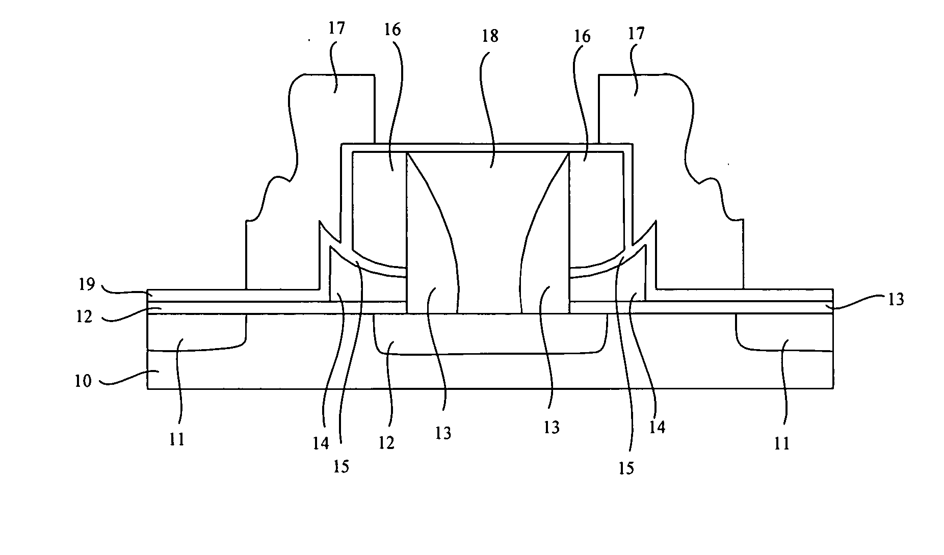
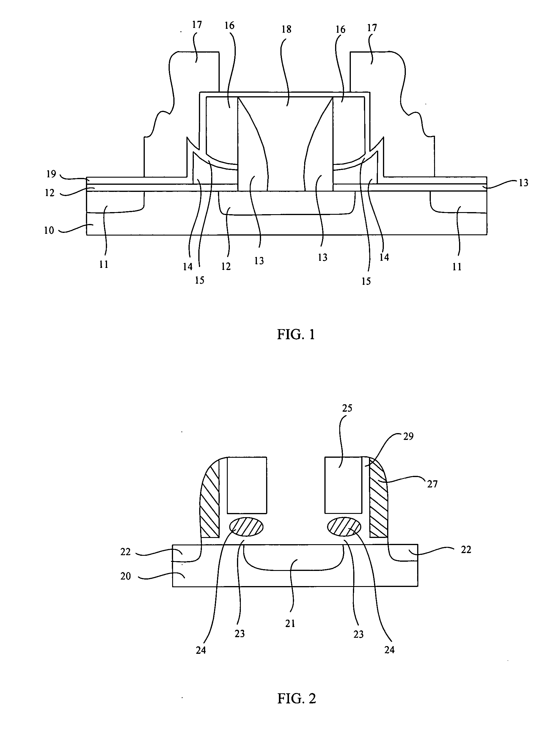
[0011] A method of forming a split-gate effect transistor comprises providing a substrate having a pair of floating gates, a first conductive material layer between said pair of floating gates, and a first dielectric layer above the first conductive material layer; forming a control gate having a second dielectric layer above said control gate, wherein the control gate is self-aligned to the pair of floating gates by using the first and second dielectric layers as an etching hard mask; and forming a pair of source/drain regions into the substrate and beside the pair of floating gates and t...

Problems solved by technology

Moreover, processes to fabricate the floating gates and control gates of the flash memory devices are very complex and often make devices fail during fabrication.
It is difficult to fabricate split-gate structure flash devices in a desired memory cell space.
Unfortunately, it is often difficult to form a pair of symmetric control gates in the memory cell.
However, it creates another problem.

Method used


Image

  • Split gate field effect transistor with a self-aligned control gate
  • Split gate field effect transistor with a self-aligned control gate
  • Split gate field effect transistor with a self-aligned control gate

Examples


Embodiment Construction

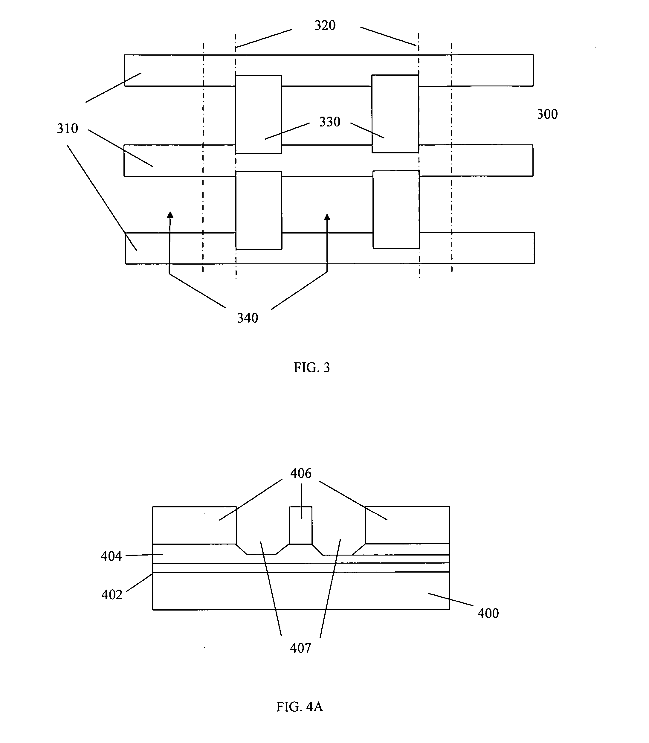
[0017] Referring to FIG. 3, it illustrates a top view of a memory array according to one embodiment of the present invention. Shallow trench isolations (STI) structures 403 are formed parallel to each other in a semiconductor substrate 400. Additionally, a pair of control gates 420 of the split gate field effect transistors are formed orthogonally to the STI structures 403. Pairs of floating gates 408 are formed beside the control gates 420 and overlap with the STI structures 403. Finally, source / drain regions 411 and 430 are formed beside the floating gates 408 and the control gates 420.

[0018] Referring to FIGS. 4A-4I, a series of schematic cross-sectional diagrams illustrate structures of the split-gate field effect transistors of FIG. 3. Moreover, a preferred embodiment of forming a pair of the split gate field effect transistors is performed according to these processes. First a substrate 400 having a pair of floating gates 404, a first conductive material layer 414 between the...


PUM


Abstract

A method of forming a split gate field effect transistor and a structure of the split gate field effect transistor are provided. The method of forming the split gate effect transistor firstly provides a substrate having a pair of floating gates, a first conductive material layer between the pair of floating gates, and a first dielectric layer above the first conductive material layer. Then a control gate is formed. The control gate has a second dielectric layer above the control gate, wherein the control gate is self-aligned to the pair of floating gates by using the first and second dielectric layers as an etching hard mask. Finally, a pair of source / drain regions are formed into said substrate and beside said pair of floating gates and said control gate.

Description

BACKGROUND OF THE INVENTION [0001] 1. Field of the Invention [0002] The present invention relates to fabrication of a split gate field effect transistor within a semiconductor integrated circuit. More particularly, the present invention relates to a method for forming the structure of the split gate field effect transistor and a structure of the split gate field effect transistor. [0003] 2. Description of the Related Art [0004] Higher level of integration of circuits is the trend in semiconductor fabrication. This purpose can be performed by shrinking device sizes on a chip. Many new techniques have been provided to accomplish the purpose. For example, the Deep Ultra-Violate (DUV) technique is popularly used to enhance the resolution of photolithography in semiconductor fabrication by using a light source having wavelength of 193 nm or 157 nm. By the development of DUV technology, semiconductor manufacturing technology has advanced to deep sub-micron processes. As to process integra...

Claims


Application Information

Patent Timeline
IPC IPC(8): H01L21/8247H01L27/115H01L29/423
CPCH01L27/115H01L29/42324H01L27/11521H10B69/00H10B41/30
Inventor CHU, WEN-TINGLIU, SHIH-CHANG
Owner TAIWAN SEMICON MFG CO LTD
Learn More