

Negative electrode for secondary cell and secondary cell using the same
- Summary
- Abstract
- Description
- Claims
- Application Information
AI Technical Summary
Benefits of technology
Problems solved by technology
Method used
Image

Examples
first embodiment
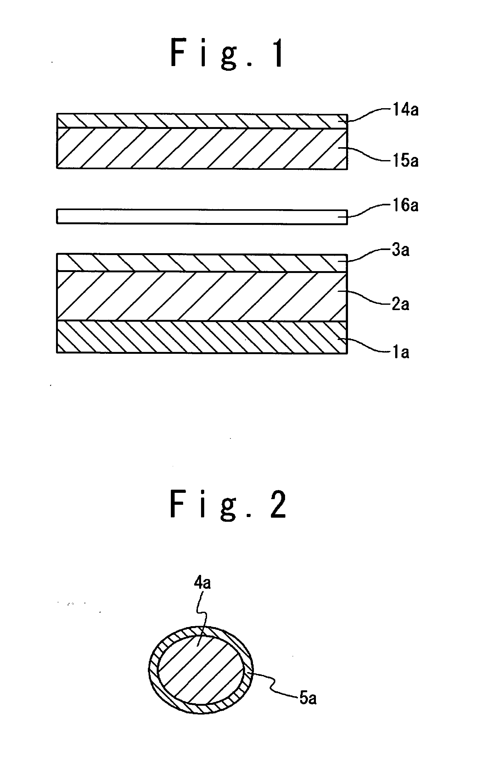
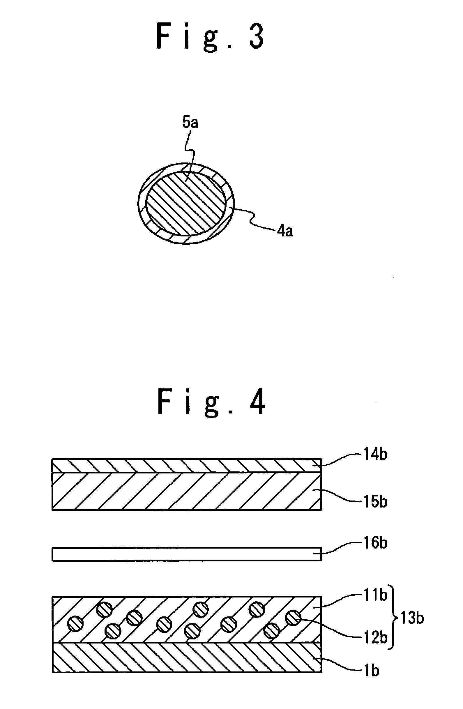
[0037]FIG. 1 is a sectional view showing a section of a secondary battery according to the first embodiment of the present invention. With reference to FIG. 1, an anode collector 1a and a cathode collector 14a are the electrodes for passing electric currents from outside in a battery and removing electric currents from a battery to outside at a time of charge and discharge. The anode collector 1a is the conductive metallic foil, which is exemplified in aluminum, copper, stainless steel, gold, tungsten, molybdenum and the like. Also, the thicknesses of the anode collector 1a and the cathode collector 14a can be set to, for example, 5 to 25 μm.
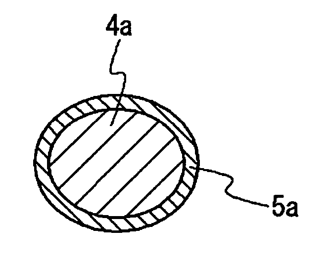
[0038] A carbon layer 2a corresponding to the first layer, which is formed on the anode collector 1a, is an anode material for absorbing and discharging the lithium in the charge and discharge. As the materials of this carbon layer 2a, the carbon materials can be listed, for example, graphite, fullerene, carbon nano-tube, DLC (Diamond-Like Carb...
second embodiment
[0050] A secondary battery according to a second embodiment of the present invention will be described in detail with reference to the drawings. FIG. 5 is a sectional view showing the section of the secondary battery according to this embodiment.
[0051] With reference to FIG. 5, the secondary battery has an anode collector 1c, a carbon layer 2c, a Li absorbing layer 3c, a Li compensating layer 6c, a cathode collector 14c, a cathode active material 15c and a separator 16c. The anode collector 1c, the carbon layer 2c, the Li absorbing layer 3c, the cathode collector 14c, the cathode active material 15c, the separator 16c and the electrolyte can be configured respectively similarly to the anode collector 1a, the carbon layer 2a, the Li absorbing layer 3a, the cathode collector 14a, the cathode active material 15a, the separator 16a and the electrolyte in the first embodiment.
[0052] The Li compensating layer 6c corresponding to the layer composed of the Li or Li compound is placed in o...
third embodiment
[0057] A secondary battery according to a third embodiment of the present invention will be described in detail with reference to the drawings. FIG. 7 is a sectional view showing a section of the secondary battery according to this embodiment.
[0058] With reference to FIG. 7, the secondary battery has an anode collector 1e, a carbon layer 2e, a Li absorbing layer 3e, a middle layer 7e, a Li compensating layer 6e, a cathode collector 14e, a cathode active material 15e and a separator 16e. The anode collector 1e, the carbon layer 2e, the Li absorbing layer 3e, the cathode collector 14e, the cathode active material 15e, the separator 16e and the electrolyte can be configured respectively similarly to the anode collector 1a, the carbon layer 2a, the Li absorbing layer 3a, the cathode collector 14a, the cathode active material 15a, the separator 16a and the electrolyte in the first embodiment. Also, the Li compensating layer 6e can be configured similarly to the Li compensating layer 6c ...
PUM
 Abstract
Description
Claims
Application Information