Deposition of carbon and nitrogen doped poly silicon films, and retarded boron diffusion and improved poly depletion

a technology of carbon and nitrogen doped poly silicon and carbon and nitrogen, which is applied in the direction of crystal growth process, coating, chemistry apparatus and processes, etc., can solve the problems of device instability, surface punching, and threshold voltage shi

Inactive Publication Date: 2005-04-21
APPLIED MATERIALS INC +1
View PDF10 Cites 34 Cited by
  • Summary
  • Abstract
  • Description
  • Claims
  • Application Information

AI Technical Summary

Problems solved by technology

However, this approach may create serious gate dopant penetration into the channel which results in threshold voltage shift, surface punch-through, and device instability.
Carbon also can be implanted in the film, although implantation damage may be caused.
The conventional films and methods for producing films have not necessarily provided all of the film characteristics that may be desirable for responding to the challenges of 90-nm and sub-90 nm technology.
Nor are there adequately simple, feasible production methodologies for making films to have desired characteristics.

Method used


Image

  • Deposition of carbon and nitrogen doped poly silicon films, and retarded boron diffusion and improved poly depletion
  • Deposition of carbon and nitrogen doped poly silicon films, and retarded boron diffusion and improved poly depletion
  • Deposition of carbon and nitrogen doped poly silicon films, and retarded boron diffusion and improved poly depletion

Examples


##ventive example 1

INVENTIVE EXAMPLE 1

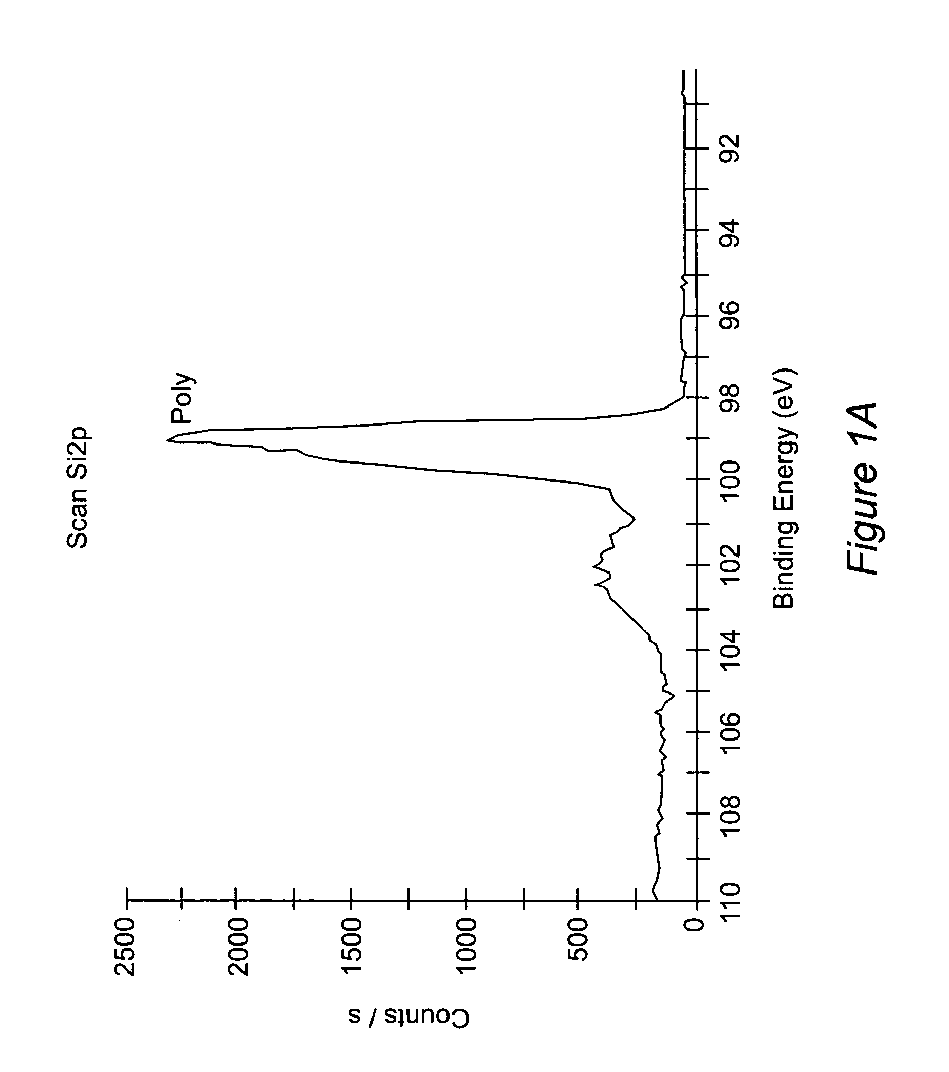
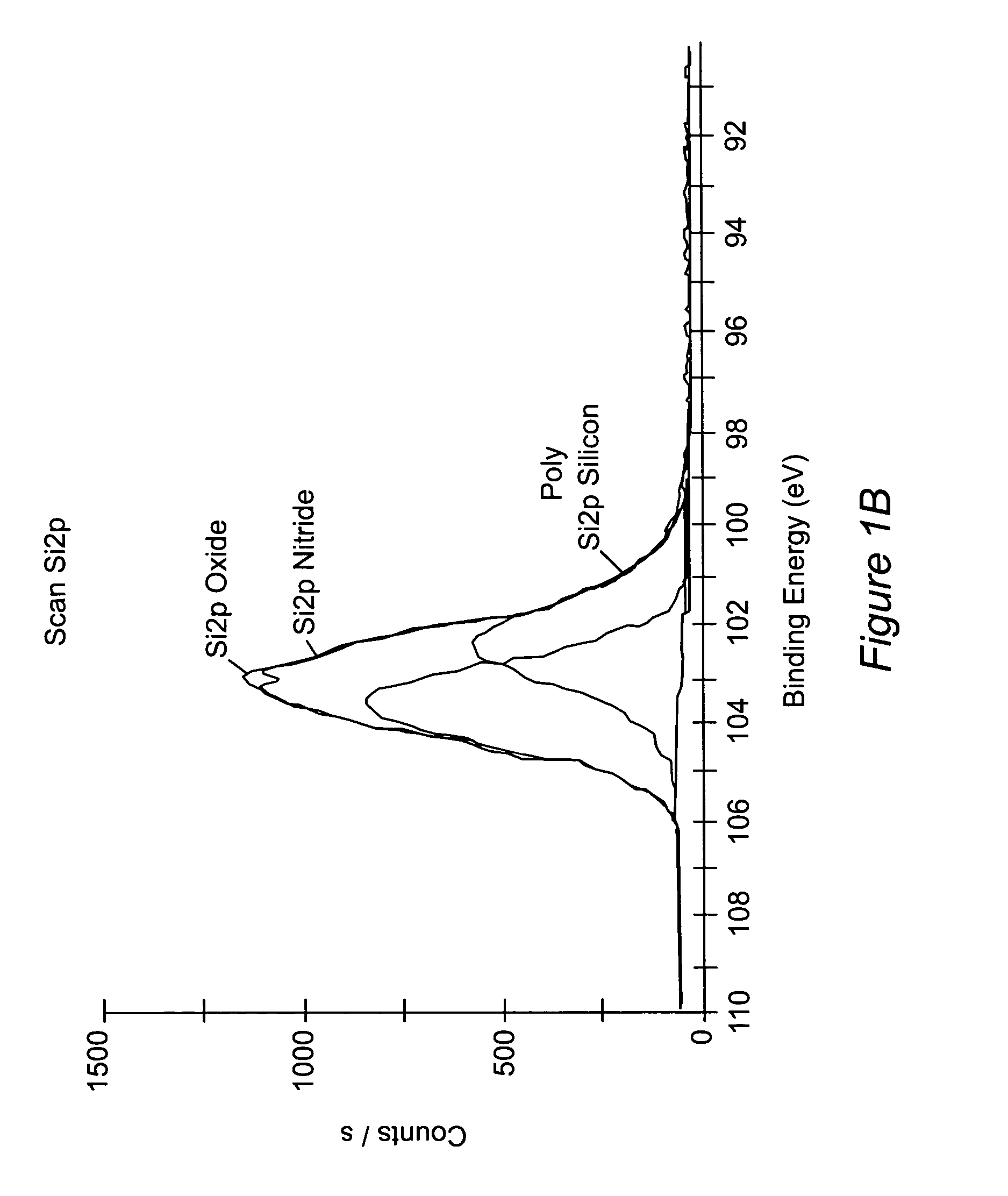
[0041] Films were produced according to the conditions and parameters set forth in Table 1 below.

TABLE 1Exp. 1Exp. 2Exp. 3Time (sec)606060Pressure (torr)100100100Heater Temp. (C.)700700700Spacing (mil)550550550Gases (sccm)N2-1800080008000N2Purge500050005000SiH4454545H2000BTBAS0200950Thickness (Angstroms)1118365179XPSPoly SiPoly SiNo Poly SiNo O, NO, NO, NAugerNo CCC

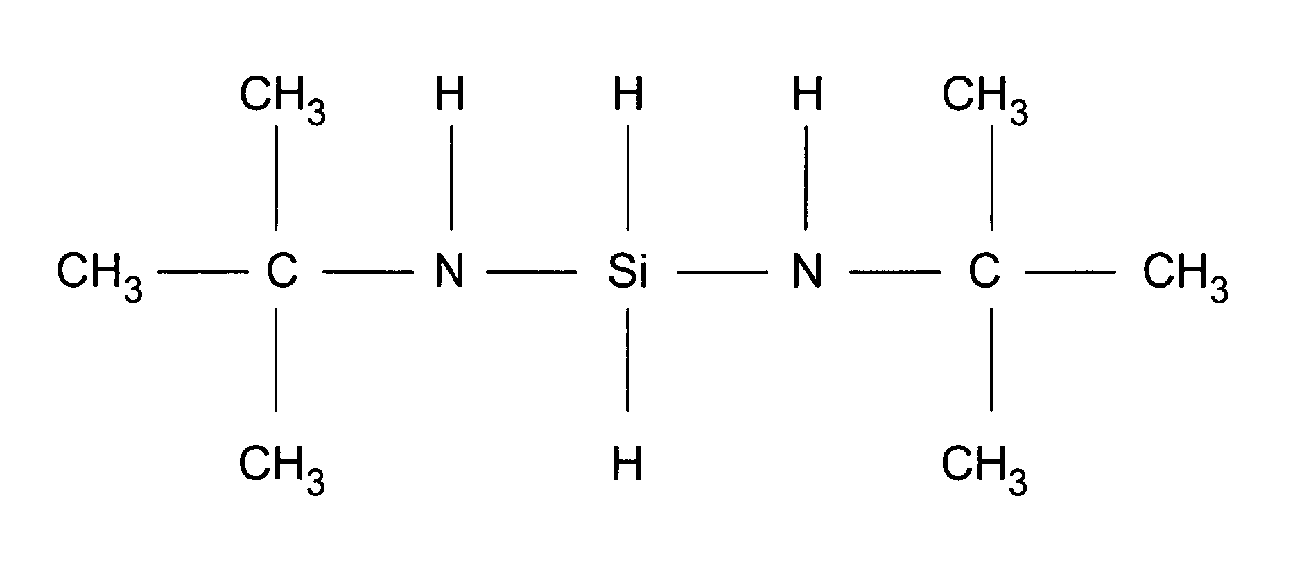
Thus, experiment 2 in Table 1 shows an example of process conditions for forming a nitrogen and carbon doped polysilicon film. XPS analysis was performed on the films produced as reported in Table 1 and the present inventors found via XPS spectra the presence of poly in a film made using BTBAS, which result demonstrates the feasibility of growing poly using an SiH4 / BTBAS mixture.

[0042] In the film production according to Table 1, reagent gases were delivered simultaneously. However, it will be appreciated that in the invention, reagent gases are not required to be delivered with simultaneous flow, b...


PUM

PropertyMeasurementUnit
sizeaaaaaaaaaa
temperatureaaaaaaaaaa
gate dielectric scalabilityaaaaaaaaaa

Abstract

A compound that includes at least Si, N and C in any combination, such as compounds of formula (R—NH)4-nSiXn wherein R is an alkyl group (which may be the same or different), n is 1, 2 or 3, and X is H or halogen (such as, e.g., bis-tertiary butyl amino silane (BTBAS)), may be mixed with silane or a silane derivative to produce a film. A polysilicon silicon film may be grown by mixing silane (SiH4) or a silane derviative and a compound including Si, N and C, such as BTBAS. Films controllably doped with carbon and/or nitrogen (such as layered films) may be grown by varying the reagents and conditions.

Description

BACKGROUND OF THE INVENTION [0001] 1. Field of the Invention [0002] The present invention generally relates to integrated circuit manufacture, and more particularly to thin films and their production. [0003] 2. Background Description [0004] In logic technologies at a size of 90 nm and smaller, the quality and characteristics of polysilicon is a major factor in determining the gate dielectric scalability. In order to reduce depletion capacitance of gate polysilicon, higher doping concentration at the polysilicon and gate oxide interface has been strongly required. This requirement has been met by increasing poly dopant dose and higher temperature activation. However, this approach may create serious gate dopant penetration into the channel which results in threshold voltage shift, surface punch-through, and device instability. [0005] In recent literature, L. Jalabert et al., “Reduction of boron penetration through thin silicon oxide with a nitrogen doped silicon layer, “Microelectron...

Claims


Application Information

Patent Timeline
Patent Type & Authority Applications(United States)
IPC IPC(8): C23C16/24C23C16/36C30B1/00H01L21/20H01L21/205H01L21/36
CPCC23C16/24H01L21/0262H01L21/02532C23C16/36
Inventor CHAKRAVARTI, ASHIMA B.MADAN, ANITALEE, WOO-HYEONGDIBELLO, GREGORY WAYNEIYER, RAMASESHAN SURYANARAYANAN
Owner APPLIED MATERIALS INC
Why Eureka
Try Eureka