Electron beam lens for micro-column electron beam apparatus and method of fabricating the same

a micro-column electron beam and electron beam technology, applied in the manufacture of electrode systems, electric discharge tubes/lamps, instruments, etc., can solve the problems of poor reproducibility of conventional methods of manufacturing electron beam lenses, difficult parallel arrangement of conductive thin films and in-line alignment of holes, and difficulty in ensuring the accuracy of electron beam lens manufacturing, etc., to achieve the effect of superior performan

Inactive Publication Date: 2005-04-28
ELECTRONICS & TELECOMM RES INST
View PDF3 Cites 21 Cited by
  • Summary
  • Abstract
  • Description
  • Claims
  • Application Information

AI Technical Summary

Benefits of technology

[0010] The present invention provides an electron beam lens which provides a superior performance since thin conductive films are arranged in parallel, holes are correctly self-aligned, and holes have uniform shapes.

Problems solved by technology

However, in the prior art, parallel arrangement of the conductive thin films and the in-line alignment of the holes is very difficult because each conductive film is separately manufactured and stacked.
Particularly, a required bonding technique is very complicated and troublesome.
Therefore, the conventional method of manufacturing an electron beam lens has poor reproducibility and produces lenses with a weak mechanical structure.

Method used


Image

  • Electron beam lens for micro-column electron beam apparatus and method of fabricating the same
  • Electron beam lens for micro-column electron beam apparatus and method of fabricating the same
  • Electron beam lens for micro-column electron beam apparatus and method of fabricating the same

Examples


Embodiment Construction

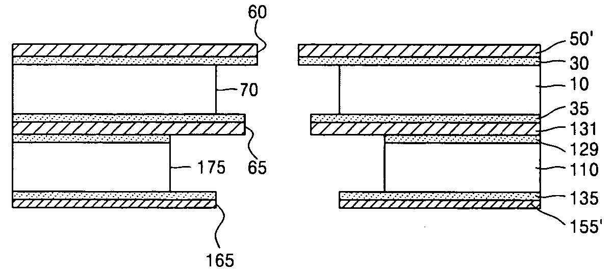
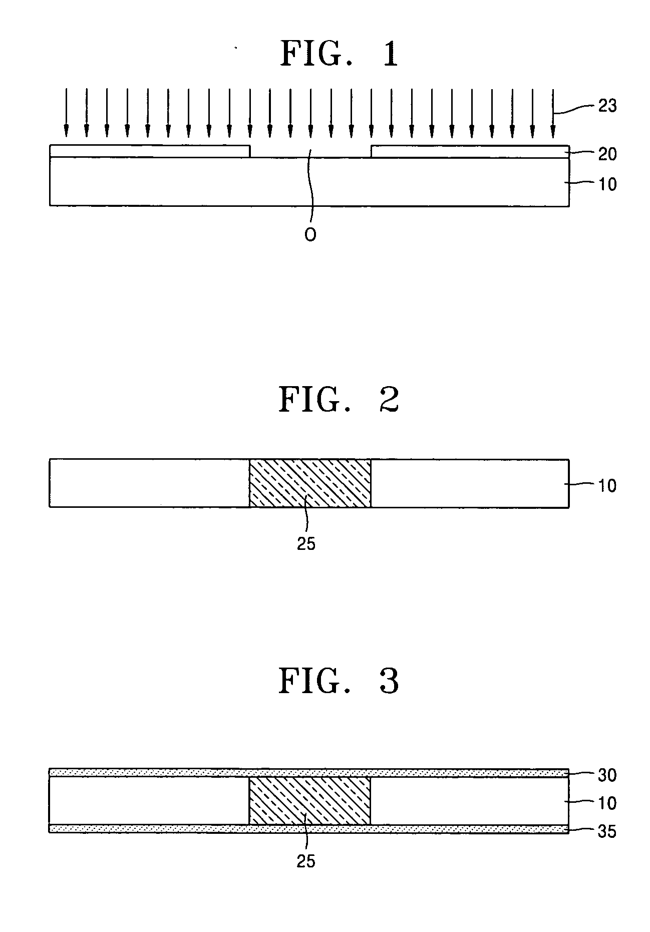
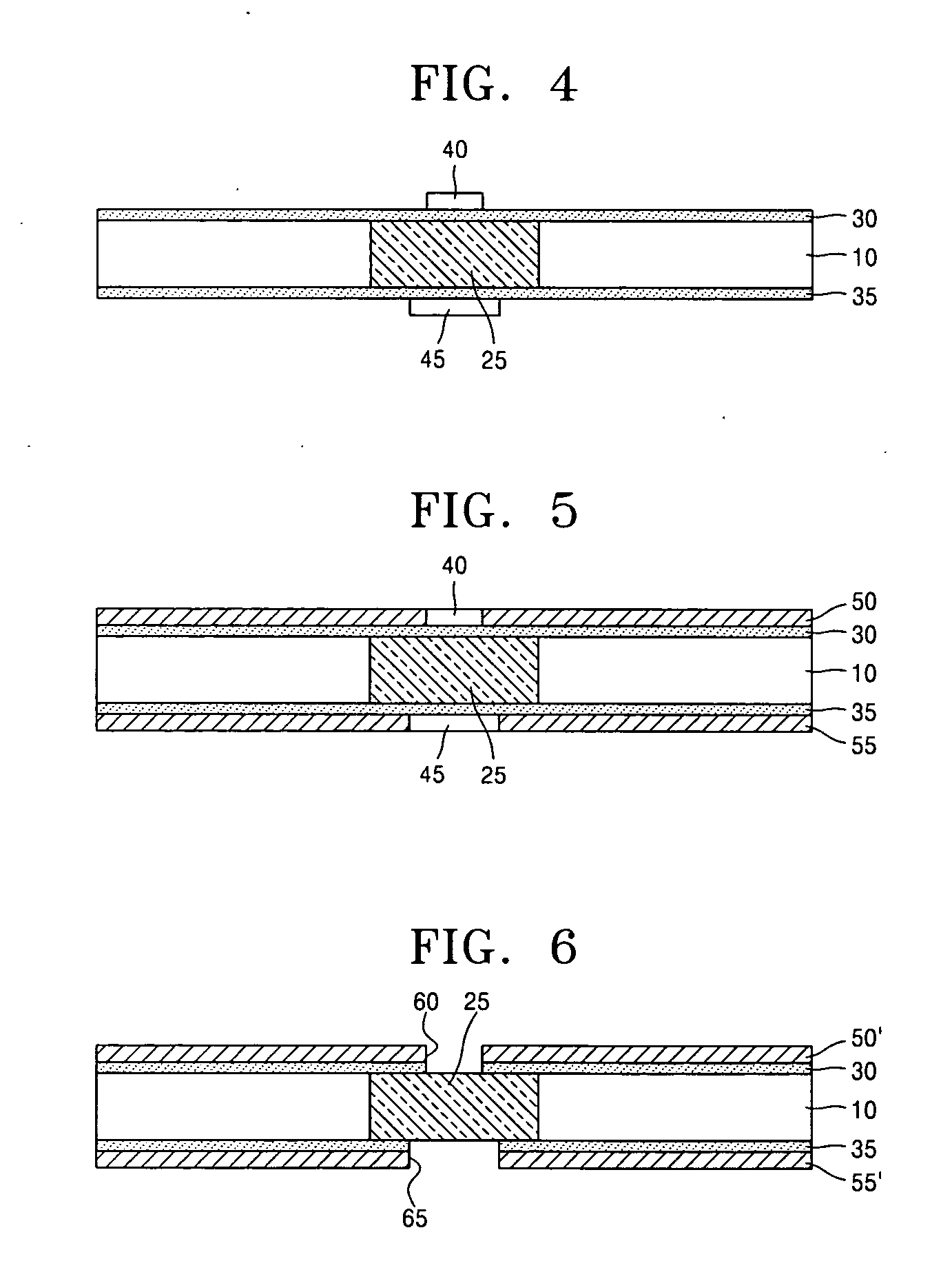
[0022] Hereinafter, exemplary embodiments of the present invention will be described more fully with reference to the accompanying drawings. This invention may, however, be embodied in many different forms and should not be construed as being limited to the embodiments set forth herein. Rather, these embodiments are described herein so that this disclosure will be thorough, complete, and fully convey the concept of the invention to those skilled in the art. In the drawings, the thicknesses of films and regions may be exaggerated for clarity. To facilitate understanding, identical reference numerals have been used, where possible, to designate identical elements that are common to the figures.

[0023] In an exemplary embodiment of the present invention, a method of manufacturing an electron beam lens with a structure including three thin metal films and two base isolation substrates, which is a representative structure of a source lens and a focus lens, will be described. However, it ...


PUM

PropertyMeasurementUnit
thicknessaaaaaaaaaa
thicknessaaaaaaaaaa
side lengthaaaaaaaaaa

Abstract

Provided is an electron beam lens for a micro-column electron beam apparatus and a method of manufacturing the same. A photosensitive glass substrate is used as a base isolation substrate and a thin metal film is grown by a plating method. Holes through which electron beam passes are formed by a lift off method after forming a resist pattern shaped as a hole on a seed metal layer and plating the thin metal film.

Description

BACKGROUND OF THE INVENTION [0001] This application claims the priority of Korean Patent Application No. 2003-74927 filed on Oct. 25, 2003, in the Korean Intellectual Property Office, the disclosure of which is incorporated herein in its entirety by reference. [0002] 1. Field of the Invention [0003] The present invention relates to an electron beam lens of a micro-column electron beam apparatus used for an electron beam exposure process of a semiconductor manufacturing process and a method of fabricating the same. [0004] 2. Description of the Related Art [0005] A micro-column electron beam apparatus is used for patterning a semiconductor device as designed by focusing an electron beam generated at a cathode onto a resist film coated on a semiconductor wafer or a mask. The micro-column electron beam apparatus includes a deflector and electron beam lenses such as a source lens and a focus lens. [0006] A deflector disposed between the electron beam lenses of the micro-column electron b...

Claims


Application Information

Patent Timeline
Patent Type & Authority Applications(United States)
IPC IPC(8): G02B3/00H01J1/02H01J3/18H01J9/02H01J9/14H01J37/12
CPCH01J3/18H01J9/02H01J9/14Y10T29/49117H01J2237/1205H01J2237/3175H01J2237/31754H01J37/12G02B3/00
Inventor CHOI, SANG KUKKIM, DAE YONG
Owner ELECTRONICS & TELECOMM RES INST
Why Eureka
Try Eureka