

Semiconductor device and fabrication method for the same
a semiconductor and fabrication method technology, applied in the direction of optics, transistors, instruments, etc., can solve the problems of avoiding conventional techniques, failing to align components in desired positions, and avoiding alignment of components, so as to achieve high reliability and accurate alignment
- Summary
- Abstract
- Description
- Claims
- Application Information
AI Technical Summary
Benefits of technology
Problems solved by technology
Method used
Image

Examples
first embodiment
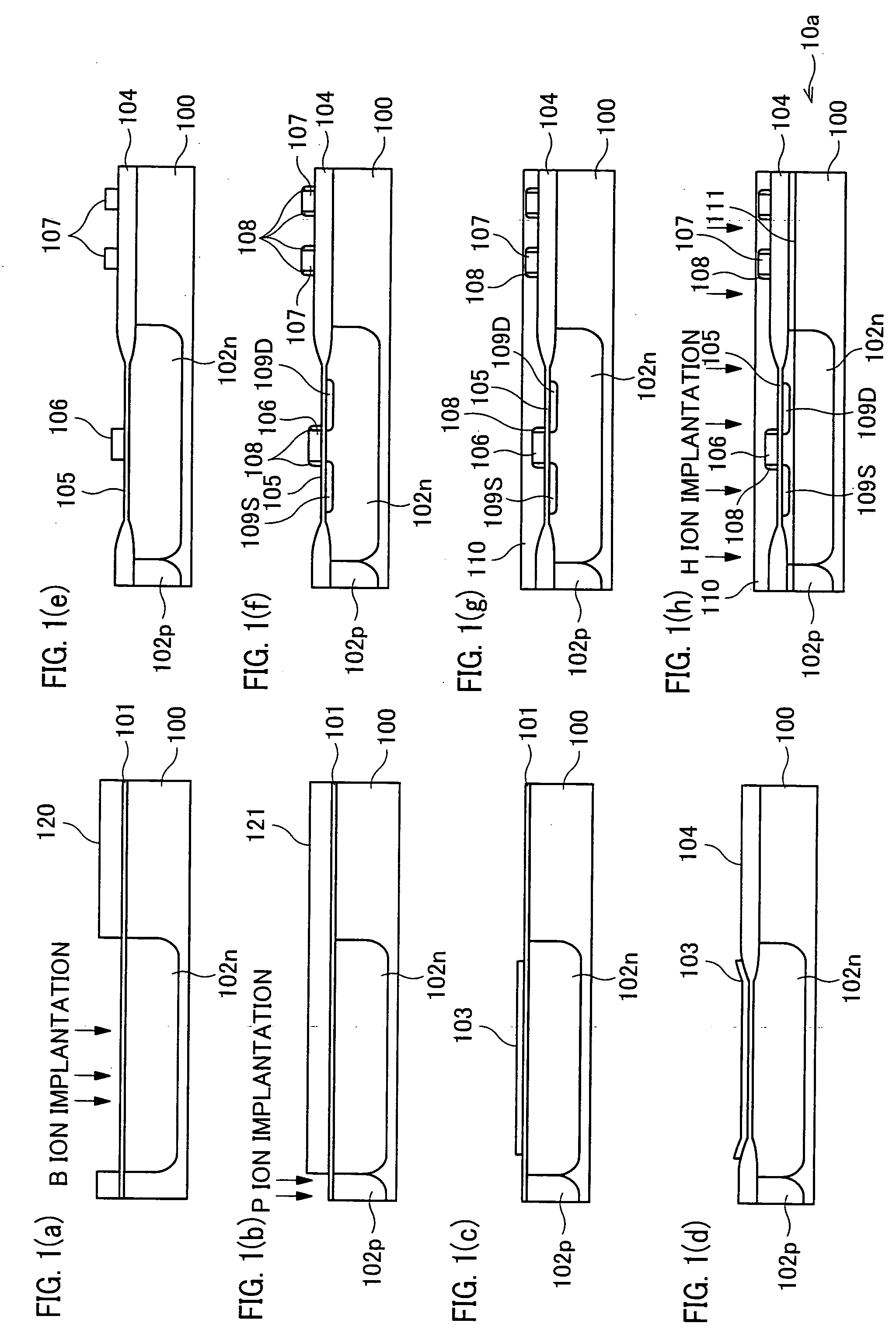
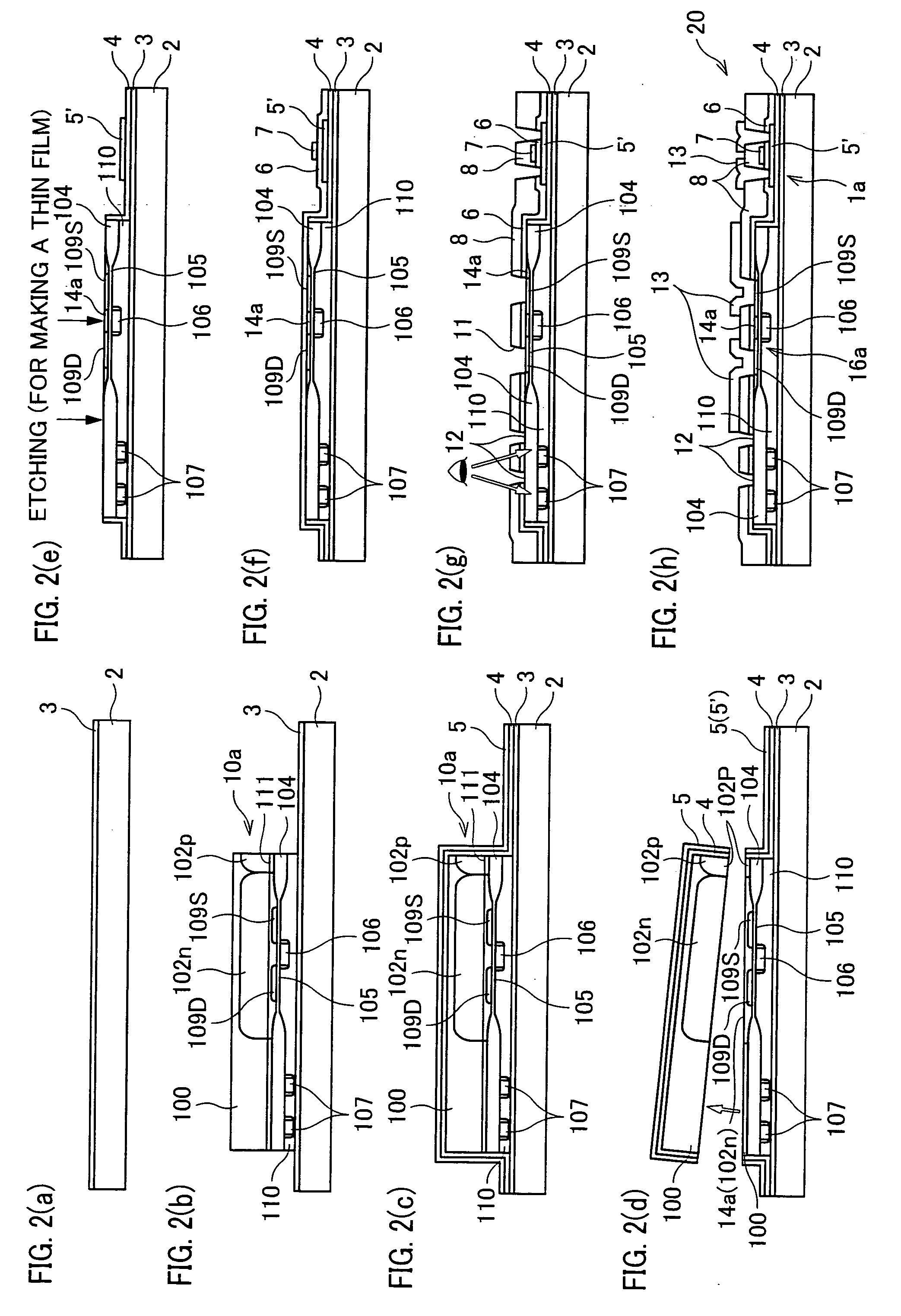
[0030] [First Embodiment]
[0031] One embodiment of the present invention is described below with reference to Figures.
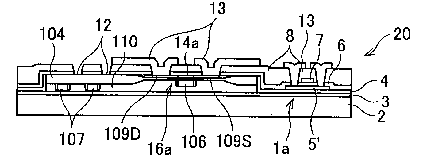
[0032] As described herein, a semiconductor device 20 of the present embodiment provides improved performance and improved functionality by forming a MOS (Metal Oxide Semiconductor) non-monocrystalline Si thin film transistor (deposited device, second device) and a MOS monocrystalline Si thin film transistor (transferred device, first device) in different regions on an insulating substrate. As described in this embodiment, the semiconductor device 20 is formed on an active-matrix substrate using TFT.
[0033] The MOS thin film transistor is a common transistor including an active semiconductor layer, a gate electrode, a gate insulating film, and dense impurity doped regions (source electrodes and drain electrodes) formed on the both sides of a gate, wherein the gate electrode adjusts the carrier density of the semiconductor layer beneath the gate, so as to adjust a flo...
second embodiment
[0099] [Second Embodiment]
[0100] Another embodiment of the present invention is explained below with reference to the figures.
[0101] In the first embodiment above, the element isolation was realized by Locos Oxidization (field oxide film (SiO2 film) 104); however, there are some alternatives. For example, element isolation may be realized by shallow trench isolation (trench isolation), in which the alignment mark is formed on the filled hole of the trench section.
[0102] The present embodiment explains a semiconductor device and a fabrication method thereof, in which the element isolation of the monocrystalline Si substrate is realized by trench isolation.
[0103] The present embodiment uses a semiconductor device 20b that is the same as the semiconductor device 20 above, except for a monocrystalline Si substrate 10b having different structure of the element-isolation region from that of the monocrystalline Si substrate 10a. For ease of explanation, materials having the equivalent f...
third embodiment
[0146] [Third Embodiment]
[0147] Still another embodiment of the present invention is explained below with reference to the figures. FIGS. 5(a) through 5(k) are cross-sectional views illustrating manufacturing steps according to the present embodiment in which a monocrystalline Si substrate 10c is transferred on the insulating substrate 2. FIGS. 6(a) through 6(h) are cross-sectional views illustrating other manufacturing steps of a semiconductor device according to the present embodiment.
[0148] In the first and second embodiments, the alignment mark 107 is formed from a polysilicon, which is also used for the gate electrode 106. However, any material allowing detection by light may be used.
[0149] The present embodiment explains a semiconductor device including an alignment mark 114 formed from the same metal material as that used for metal leads 113 formed on the monocrystalline Si substrate 10c, and also explains the manufacturing method thereof.
[0150] The present embodiment uses...
PUM
 Abstract
Description
Claims
Application Information