Recess gate transistor structure for use in semiconductor device and method thereof

a semiconductor device and gate transistor technology, applied in the field ofmos transistors, can solve the problems of short channel effect, leakage current, other difficulties, increase load capacity, etc., and achieve the effects of reducing load capacity, reducing contact region, and reducing gate induced drain leakage (gidl)

Inactive Publication Date: 2005-04-28
SAMSUNG ELECTRONICS CO LTD
View PDF12 Cites 29 Cited by
  • Summary
  • Abstract
  • Description
  • Claims
  • Application Information

AI Technical Summary

Benefits of technology

[0014] Some embodiments of the invention provide a recess gate transistor structure and method thereof, including forming an inner spacer having a predetermined thickness and depth in a sidewall of a gate that is in contact with a first active region electrically connected to an upper capacitor, so as to reduce a contact region between the first active region and the gate, and to also reduce a load capacity, thereby diminishing a gate induced drain leakage (GIDL). The structure and method also reduce a generation of leakage that is caused by a concentration of an electric field on an edge portion in contact between an upper part of the first active region and the gate by the use of the inner spacer. In addition, the structure and method make the photolithography process easy by ensuring a misalign margin by extending a length of recess longer than a length of the gate without reducing the length of the gate, and preventing a split of the gate by appropriately controlling the length of the recess.

Problems solved by technology

Thus, designing to integrate more semiconductor devices in a semiconductor chip of limited size reduces an interval between gates, causing a short channel effect, a leakage current, and other difficulties.
This causes an increased load capacity and gate induced drain leakage (GIDL).
Furthermore, a length of the recess is formed smaller than a length of the gate in order to ensure a misalign margin, and this requires a high-level of precision in the photolithography process and causes a drop in a production yield of the semiconductor device.

Method used


Image

  • Recess gate transistor structure for use in semiconductor device and method thereof
  • Recess gate transistor structure for use in semiconductor device and method thereof
  • Recess gate transistor structure for use in semiconductor device and method thereof

Examples


Embodiment Construction

[0020] The foregoing and other features and advantages of the invention will be apparent from the more particular description of exemplary embodiments of the invention, as illustrated in the accompanying drawings of FIGS. 5 to 14. The invention may be embodied in many different forms and should not be construed as being limited to the exemplary embodiments set forth herein. Rather, these exemplary embodiments are provided so that this disclosure is thorough and complete, and to convey the concept of the invention to those skilled in the art.

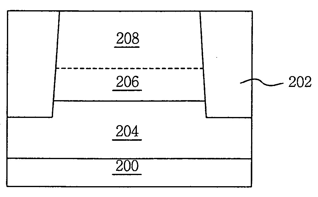
[0021] A method of forming a recess gate transistor will be described as follows, referring to FIGS. 5 through 14.

[0022] Referring to FIG. 5, a device isolation film 202, which defines an active region and a non-active region, is formed on a predetermined region of a p-type semiconductor substrate 200. A p-type impurity, e.g., Boron, is ion-implanted with an energy of 400 KeV and a density of about 2.0×10¹³ ion atoms / cm into the surface of the ...


PUM


Abstract

An inner spacer is formed in a sidewall of a gate in contact with a first active region that is electrically connected to an upper capacitor, thereby reducing a gate induced drain leakage (GIDL). A structure of a recess gate transistor includes a gate insulation layer, a gate electrode, a first gate spacer, a second gate spacer and source/drain regions. The gate insulation layer is formed within a recess. The gate electrode is surrounded by the gate insulation layer and is extended from within the recess. The first gate spacer is spaced with a predetermined distance horizontally with a portion of the gate insulation layer, being formed in a sidewall of the gate electrode. The second gate spacer is formed in another part of the sidewall of the gate electrode. The source/drain regions are formed mutually oppositely on first and second active regions with the gate electrode therebetween.

Description

CROSS REFERENCE TO RELATED APPLICATIONS [0001] This application claims priority from Korean Patent Application No. 2003-73762, filed on Oct. 22, 2003, the contents of which are hereby incorporated by reference for all purposes. BACKGROUND OF THE INVENTION [0002] 1. Field of the Invention [0003] This disclosure relates to a MOS transistor, and more particularly, to a recess gate transistor structure for use in a semiconductor device and a method thereof. [0004] 2. Description of the Related Art [0005] Techniques for the manufacture and production of semiconductor devices are being developed worldwide, based on requirements of semiconductor users and semiconductor manufacturers. The semiconductor manufacturers are giving an impetus to research and development for enhanced high-speed, miniaturized, highly-integrated, large-capacity semiconductor devices with more stabilized and smooth operation. Thus, designing to integrate more semiconductor devices in a semiconductor chip of limited ...

Claims


Application Information

Patent Timeline
Patent Type & Authority Applications(United States)
IPC IPC(8): H01L21/336H01L29/78
CPCH01L29/7834H01L29/66621H01L29/78
Inventor KIM, JI-YOUNG
Owner SAMSUNG ELECTRONICS CO LTD
Why Eureka
Try Eureka