Use of selective oxidation to form asymmetrical oxide features during the manufacture of a semiconductor device

a technology of asymmetric oxide and selective oxidation, which is applied in the direction of semiconductor devices, basic electric elements, electrical equipment, etc., can solve the problems of non-uniformity, sidewall oxidation effectively increasing the thickness of tunnel oxide, and the difference in the profile between the source and drain region, so as to reduce the problem

Inactive Publication Date: 2005-04-28
MICRON TECH INC
View PDF14 Cites 25 Cited by
  • Summary
  • Abstract
  • Description
  • Claims
  • Application Information

AI Technical Summary

Benefits of technology

[0011] The present invention provides a new method which, among other advantages, reduces problems associated with the operation of programmable read-only memory devices, particularly problems which may occur during reading and writing flash memory devices. In accordance with one embodiment of the invention the source region and drain region are doped to different doping levels, then exposed to a particular oxidizing amb...

Problems solved by technology

The sidewall oxidation effectively increases the thickness of the tunnel oxide, and does so in a non-uniform manner.
Since the oxida...

Method used


Image

  • Use of selective oxidation to form asymmetrical oxide features during the manufacture of a semiconductor device
  • Use of selective oxidation to form asymmetrical oxide features during the manufacture of a semiconductor device
  • Use of selective oxidation to form asymmetrical oxide features during the manufacture of a semiconductor device

Examples


Embodiment Construction

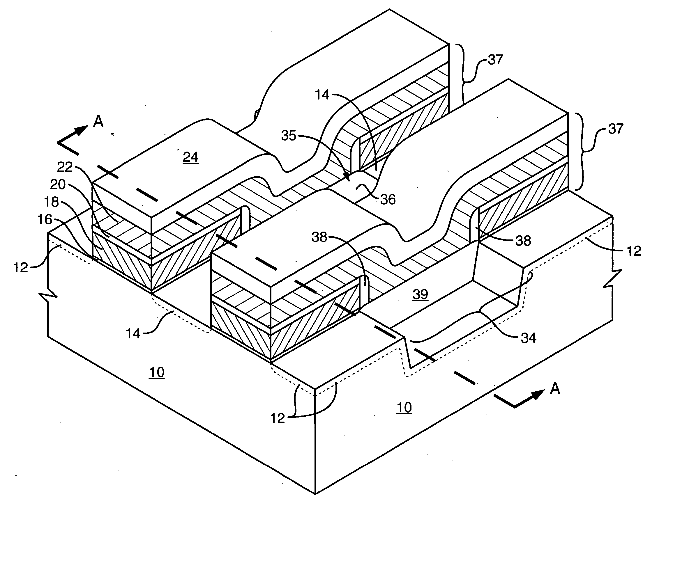
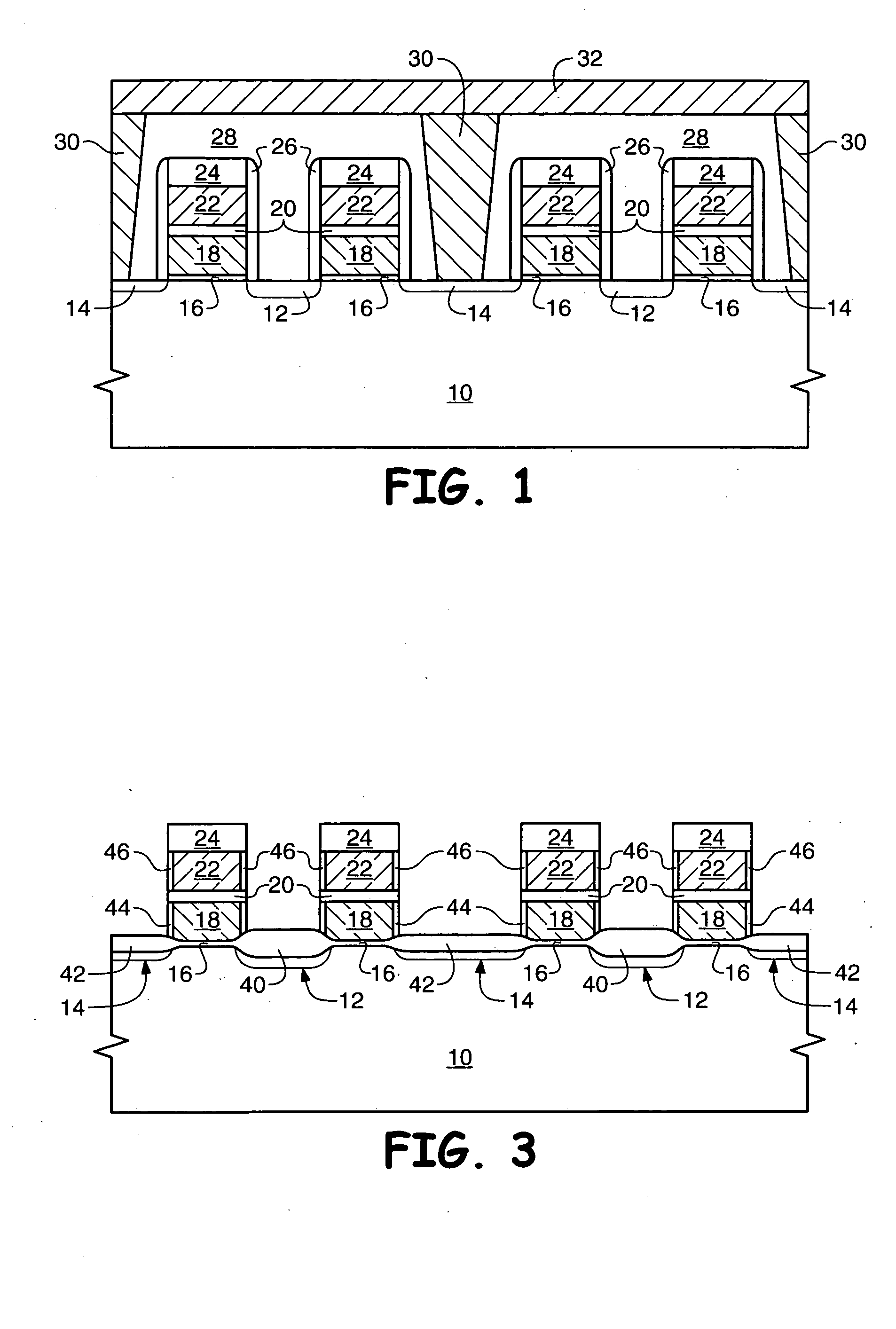
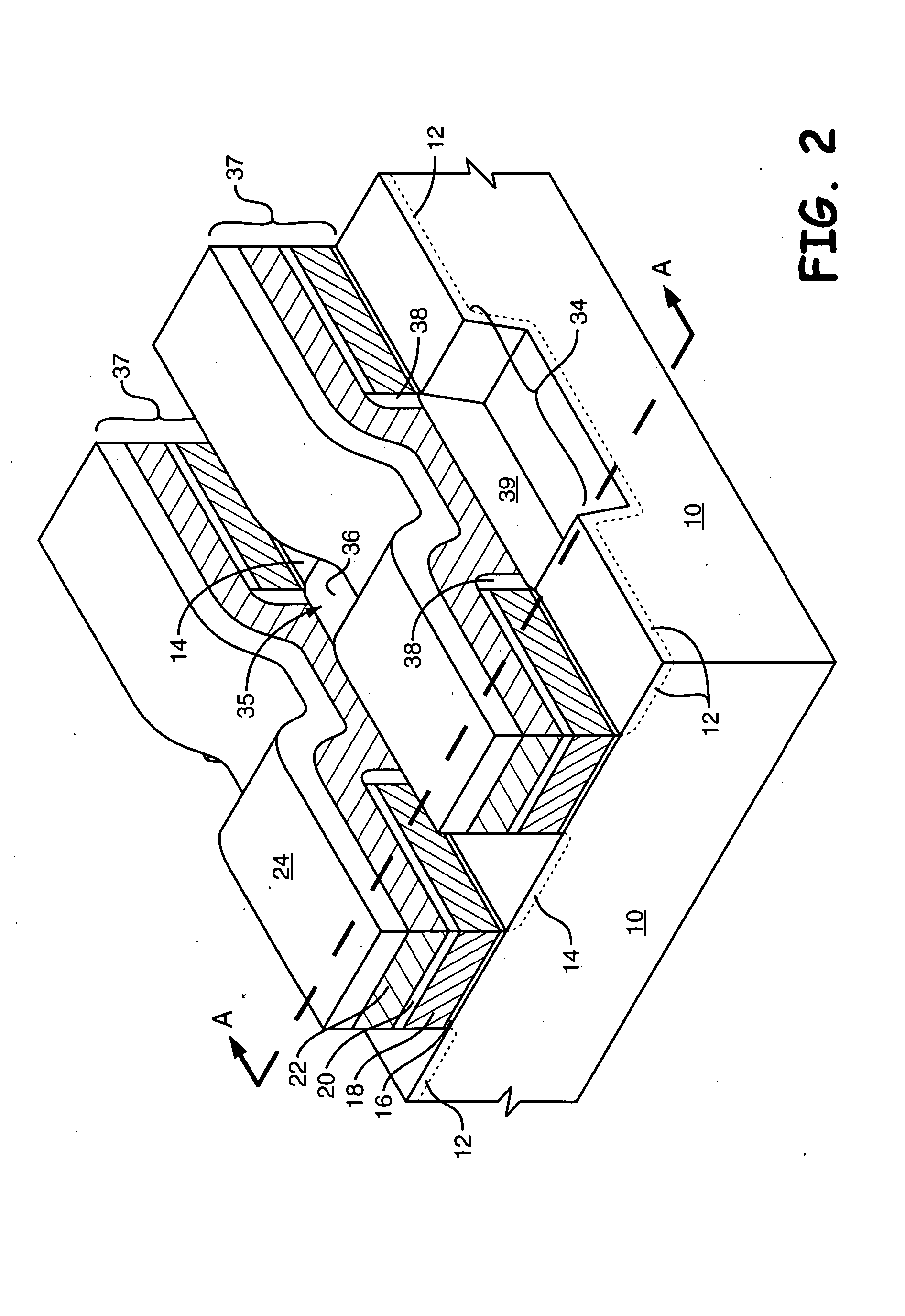
[0022] The term “wafer” is to be understood as a semiconductor-based material including silicon, silicon-on-insulator (SOI) or silicon-on-sapphire (SOS) technology, doped and undoped semiconductors, epitaxial layers of silicon supported by a base semiconductor foundation, and other semiconductor structures. Furthermore, when reference is made to a “wafer” in the following description, previous process steps may have been utilized to form regions or junctions in or over the base semiconductor structure or foundation. Additionally, when reference is made to a “substrate assembly” in the following description, the substrate assembly may include a wafer with layers including dielectrics and conductors, and features such as transistors, formed thereover, depending on the particular stage of processing. Further, in the discussion and claims herein, the term “on” used with respect to two layers, one “on” the other, means at least some contact between the layers, while “over” means the laye...


PUM


Abstract

A sidewall oxidation process for use during the formation of a transistor such as a flash memory cell allows for improved control of a gate oxide profile. The method comprises doping transistor source and drain regions to different doping levels, then performing a transistor sidewall oxidation using a particular process to modify the gate oxide thickness. The oxide forms at a faster rate along the source sidewall than along the drain sidewall. By using ranges within the oxidation environment described, a source side gate oxide having a variable and selectable thickness may be formed, while forming a drain-side oxide which has a single thickness where a thinner layer is desirable. This leads to improved optimization of key competing requirements of a flash memory cell, such as program and erase performance, while maintaining sufficient long-term data retention. The process may allow improved cell scalability, shortened design time, and decreased manufacturing costs.

Description

FIELD OF THE INVENTION [0001] This invention relates to the field of semiconductor manufacture and, more particularly, to a method for forming an asymmetrical gate oxide layer during the formation of a transistor on a semiconductor device such as a flash memory device. BACKGROUND OF THE INVENTION [0002] Floating gate memory devices such as flash memories include an array of electrically-programmable and electrically-erasable memory cells. Typically, each memory cell comprises a single n-channel metal oxide semiconductor (NMOS) transistor including a floating gate interposed between a control (input) gate and a transistor channel region. A layer of high-quality tunnel oxide used as gate oxide separates the transistor channel and the floating gate, and an oxide-nitride-oxide (ONO) dielectric stack separates the floating gate from the control gate. The ONO stack typically comprises a layer of silicon nitride (Si3N4) interposed between underlying and overlying layers of silicon dioxide ...

Claims


Application Information

Patent Timeline
IPC IPC(8): H01L21/316H01L21/321H01L21/336H01L21/8238H01L21/8247H01L27/115
CPCH01L21/02238H01L21/02255H01L21/31662Y10S438/981H01L27/115H01L27/11521H01L21/32105H10B69/00H10B41/30
Inventor RUDECK, PAUL J.POWELL, DON C.
Owner MICRON TECH INC
Why Eureka
Try Eureka