Check patentability & draft patents in minutes with Patsnap Eureka AI!

Optical sensor, method of manufacturing and driving an optical sensor, method of detecting light intensity

Inactive Publication Date: 2005-05-05
SANYO ELECTRIC CO LTD
View PDF3 Cites 27 Cited by
  • Summary
  • Abstract
  • Description
  • Claims
  • Application Information

AI Technical Summary

Benefits of technology

[0015] Also, since a carbon nanotube, which is highly conductive, is employed in the optical sensor of the present invention as an interconnect material connecting the source electrode and the drain electrode, a sufficient current value can be obtained despite miniaturizing the electrodes. Consequently, the optical sensor can be made smaller in dimensions. As a result, a number of the source electrodes and the drain electrodes, i.e. a number of pixels per unit area can be made greater.
[0038] Further, according to the present invention, since light intensity is detected through applying a voltage to the carbon nanotube, detecting variation of a current value in the carbon nanotube caused by irradiation of a light to the light sensitive polarizable layer, and based on the variation of the current value, a relatively large variation of the current value can be obtained from a relatively small polarization signal, therefore a method of detecting by which light intensity can be measured with high precision and high sensitivity can be accomplished.

Problems solved by technology

However, a signal originating from an electric polarization of a photosensitive molecule such as bacteriorhodopsin is so small that a sufficient current value is not always obtainable when detecting an induced current.

Method used


Image

  • Optical sensor, method of manufacturing and driving an optical sensor, method of detecting light intensity
  • Optical sensor, method of manufacturing and driving an optical sensor, method of detecting light intensity
  • Optical sensor, method of manufacturing and driving an optical sensor, method of detecting light intensity

Examples


first embodiment

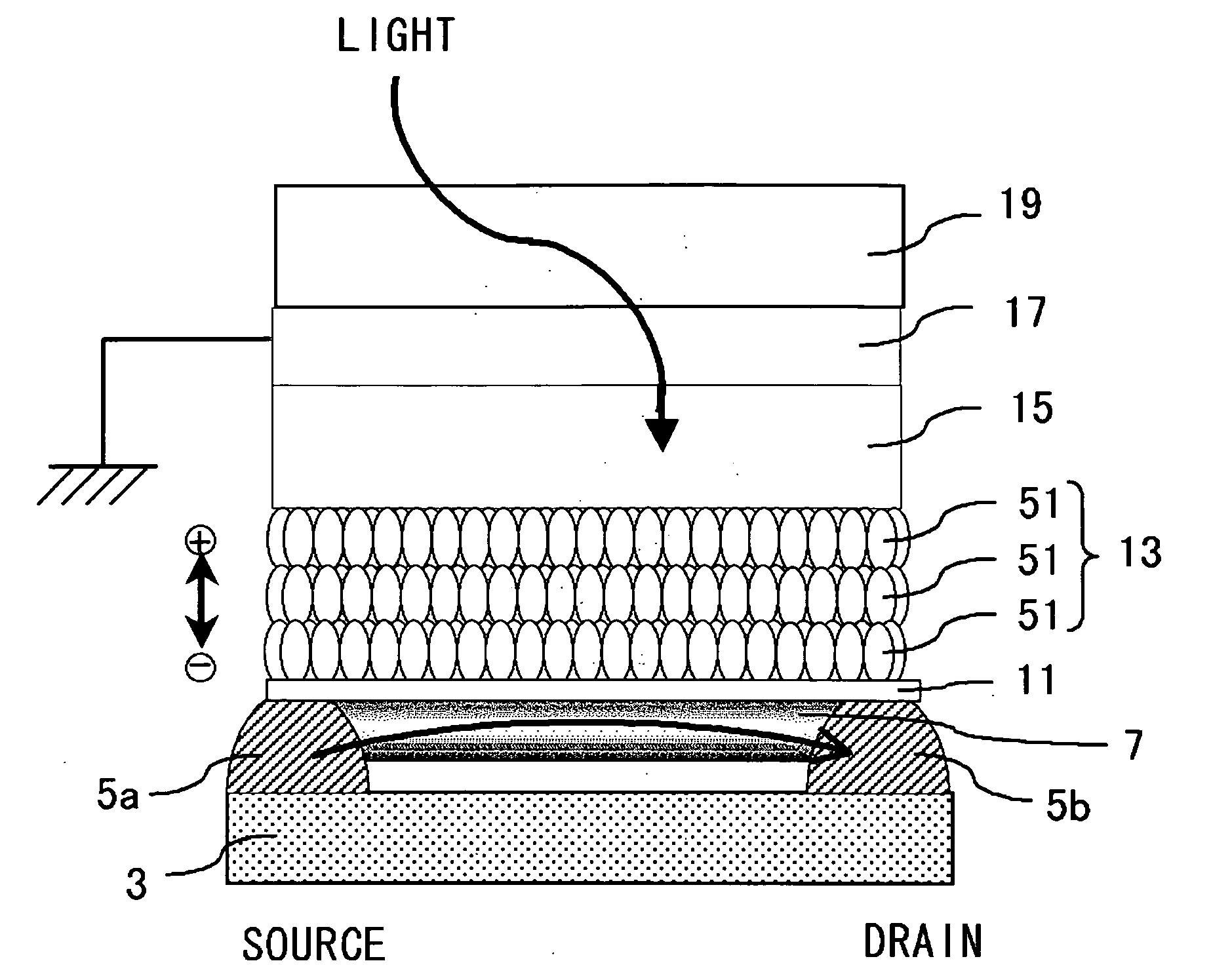
[0084] The optical sensor according to this embodiment is shown in FIGS. 2 and 3. The source electrode 5a and the drain electrode 5b connected via the carbon nanotube 7 are provided on the substrate 3, and the insulating layer 11 is formed on the respective surfaces of the source electrode 5a and the drain electrode 5b connected via the carbon nanotube 7. The carbon nanotube 7 is an SWCNT. The protein monolayer film 51 is provided on the insulating layer 11 to serve as the light sensitively polarizable layer 13. On the light sensitively polarizable layer 13, a transparent protective layer 15 is provided for protecting the light sensitively polarizable layer 13, and a transparent conductive layer 17 and a transparent substrate 19 are provided in this sequence on the protective layer 15. In FIG. 2 the transparent conductive layer 17 is grounded, while it is also possible to apply an offset voltage to the transparent conductive layer 17. In this case, for example the substrate 3 can be...

second embodiment

[0149] The step (ii) “Connecting the source electrode 5a and the drain electrode 5b with the carbon nanotube 7” of the first embodiment can be performed in the following method.

[0150] To start with, as shown in FIGS. 15A and 15B, the alignment layer of the carbon nanotube 7 is adsorbed to the substrate 3 where the source electrode 5a and the drain electrode 5b are provided in a similar manner to the first embodiment.

[0151] Then as shown in FIG. 15C, a resist layer 25 having an opening at a position corresponding to an upper portion of the source electrode 5a and the drain electrode 5b is formed. Forming the resist layer 25 can be executed by a photo-resist method, for example.

[0152] Thereafter as shown in FIG. 15D, a metal layer 27 is formed all over the substrate 3 on which the resist layer 25 is provided. A material of the metal layer 27 can be appropriately selected out of the metals or alloys that can be used for the source electrode 5a and the drain electrode 5b. The source ...

third embodiment

[0155] The step (ii) “Connecting the source electrode 5a and the drain electrode 5b with the carbon nanotube 7” of the first embodiment can be performed in the following method.

[0156] Still another method of connecting the source electrode 5a and the drain electrode 5b with the carbon nanotube 7 includes spreading a dispersion of the carbon nanotube 7 over the substrate 3 on which the source electrode 5a and the drain electrode 5b are provided, and moving an appropriate carbon nanotube 7 to a predetermined position with a probe of an AFM or the like.

[0157] As a result, the carbon nanotube 7 can be more precisely disposed between the source electrode 5a and the drain electrode 5b.


PUM


Abstract

In an optical sensor provided with an optically polarizable molecule, a pair of source electrode and drain electrode is electrically connected via a carbon nanotube. When a photosensitive molecule constituting the light sensitively polarizable layer polarizes upon receiving a light, conductance of the carbon nanotube varies. Since the variation of the conductance of the carbon nanotube incurs a variation of current value between the source electrode and the drain electrode, such variation is to be detected. Also, by forming a layer including the aligned, efficient connection with the source electrode and the drain electrode can be simply achieved. A small-sized optical sensor capable of performing with high precision and high sensitivity, manufacturing and driving method of such optical sensor, and method of light intensity detection are accomplished.

Description

[0001] This is a Continuation-in-part of International Application No. PCT / JP2003 / 009577, filed on Jul. 29, 2003. [0002] This application is based on the Japanese Patent Application No. 2002-225,291, the Japanese Patent Application No. 2002-261,244, and the Japanese Patent Application No. 2002-324,373, the content of which is incorporated hereinto by reference.BACKGROUND OF THE INVENTION [0003] 1. Field of the Invention [0004] The present invention relates to an optical sensor, method of manufacturing and driving an optical sensor, and to method of detecting light intensity. [0005] 2. Description of the Related Art [0006] Recently, demand for miniaturization and upgrading in sensitivity of an optical sensor has been remarkably increasing, and development of an optical sensor capable of detecting an optical signal through efficient conversion thereof to an electric signal has been eagerly longed for. [0007] In view of such demand the present inventors have been developing a sensor in...

Claims


Application Information

Patent Timeline
IPC IPC(8): H01J1/62H01J63/04
CPCB82Y10/00Y02E10/549H01L51/428H10K30/65
Inventor SUGIYAMA, YUKIHIRO
Owner SANYO ELECTRIC CO LTD
Features
  • R&D
  • Intellectual Property
  • Life Sciences
  • Materials
  • Tech Scout
  • Unparalleled Data Quality
  • Higher Quality Content
  • 60% Fewer Hallucinations
Learn More