Semiconductor devices having different gate dielectrics and methods for manufacturing the same

Inactive Publication Date: 2005-05-12
SAMSUNG ELECTRONICS CO LTD
View PDF15 Cites 176 Cited by
  • Summary
  • Abstract
  • Description
  • Claims
  • Application Information

AI Technical Summary

Benefits of technology

[0013] In accordance with these and other aspects of embodiments of the present invention, adequate capacitance can be accomplished in the transistor devices, for example, in NMOS and PMOS devices, while mitigating the negative impact of bulk traps and/or interface traps. These advantages can be accomplished by a first high-k layer and a second high-k layer having materials with dielectric constants of 8 or more. Also, this may be accomplished by the first high-k laye

Problems solved by technology

Unfortunately, however, at around this thickness, the use of SiO2 as a gate dielectric becomes limited.
The result is increased leakage current and increased power consumption.
However, the use of high-k dielectrics

Method used


Image

  • Semiconductor devices having different gate dielectrics and methods for manufacturing the same
  • Semiconductor devices having different gate dielectrics and methods for manufacturing the same
  • Semiconductor devices having different gate dielectrics and methods for manufacturing the same

Examples


Example

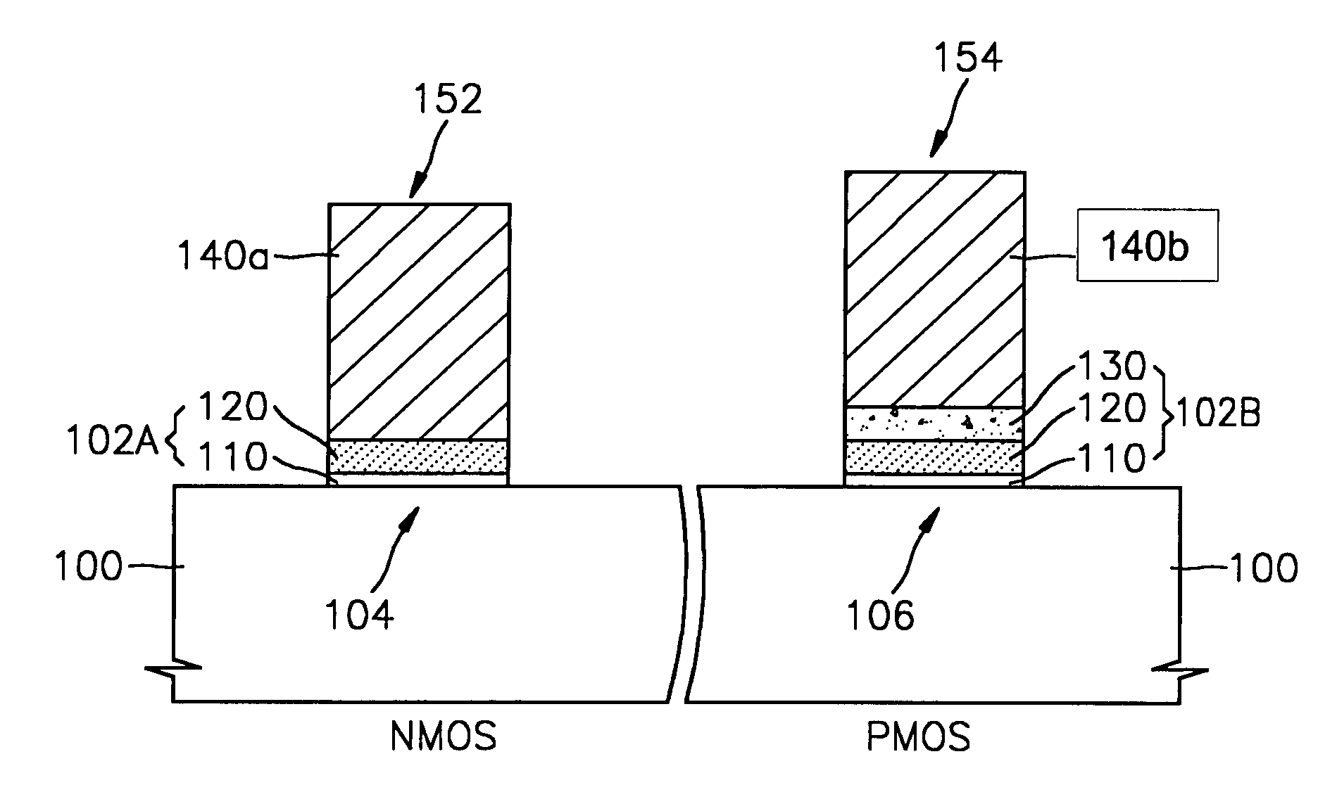
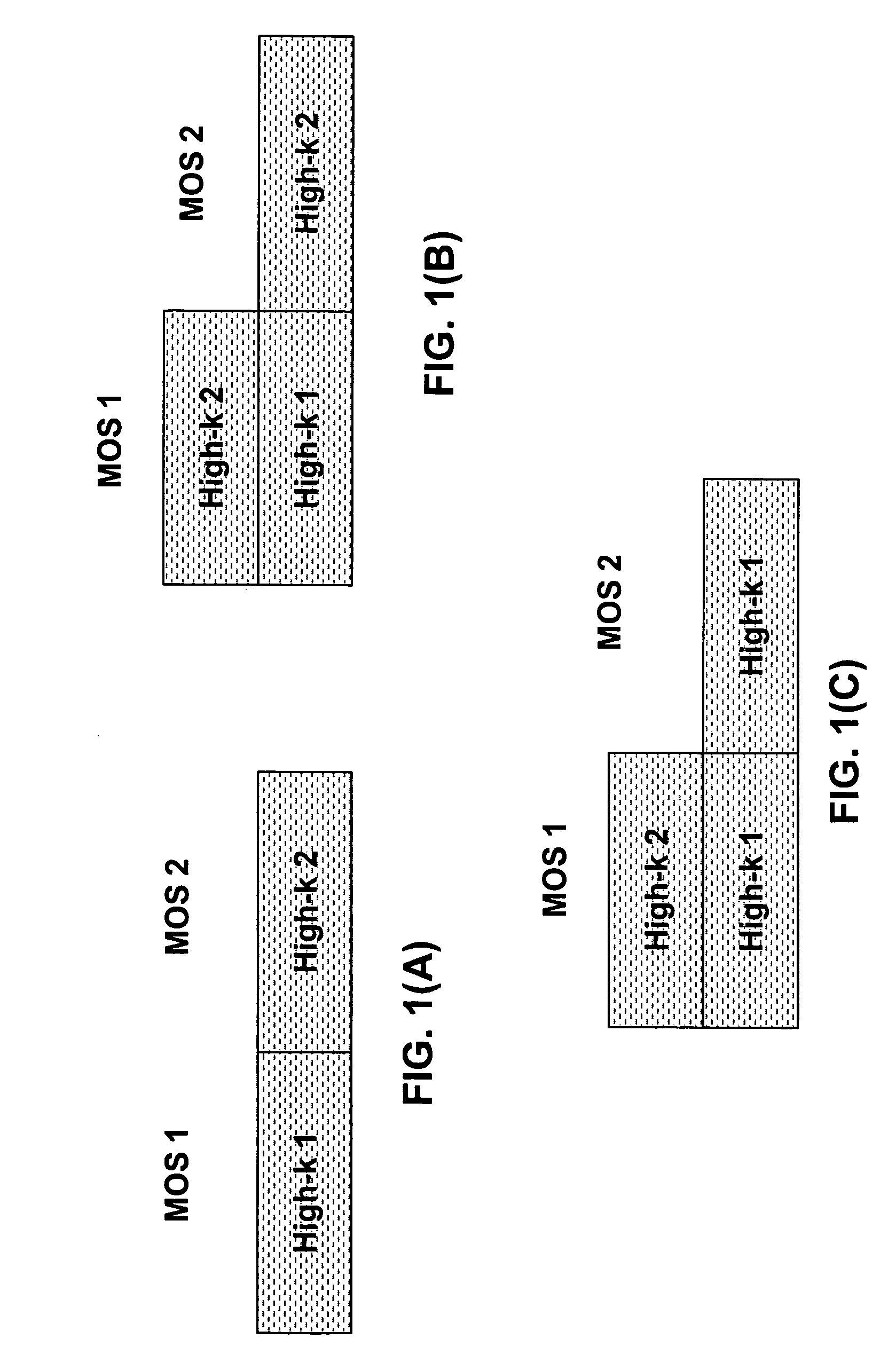
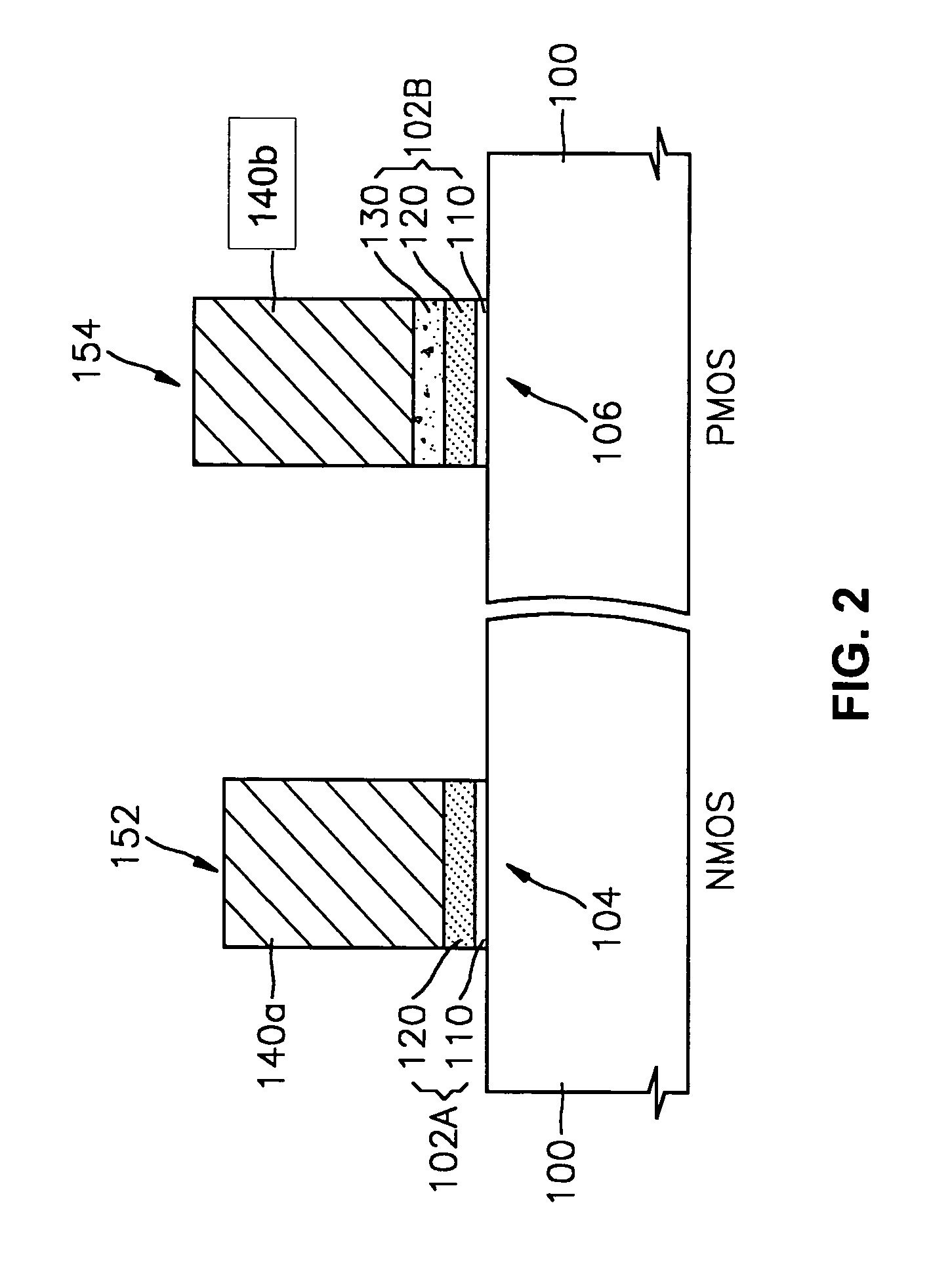
[0027] The present invention will now be described with reference to the drawings by way of several preferred but nonlimiting embodiments. It is noted that relative dimensions as illustrated in the drawings may not scale to actual dimensions.

[0028] FIGS. 1(A), 1(B) and 1(C) are simplified conceptual illustrations of embodiments of gate dielectrics used in MOS devices according to the present invention.

[0029]FIG. 1(A) illustrates the gate dielectrics of a semiconductor device including a first type of metal-oxide-semiconductor (MOS 1) and a second type of metal-oxide-semiconductor device (MOS 2). In some embodiments, MOS 1 is an n-channel metal-oxide-semiconductor (NMOS) device and MOS 2 is a p-channel metal-oxide-semiconductor (PMOS) device. In other embodiments, MOS 1 is a PMOS device and MOS 2 is an NMOS device. In the example of FIG. 1(A), the gate dielectric of MOS 1 is a first high-k dielectric material (High-k 1), and the gate dielectric of MOS 2 is a second high-k dielectri...


PUM


Abstract

A semiconductor device includes first and second transistor devices. The first device includes a first substrate region, a first gate electrode, and a first gate dielectric. The first gate dielectric is located between the first substrate region and the first gate electrode. The second device includes a second substrate region, a second gate electrode, and a second gate dielectric. The second gate dielectric is located between the second substrate region and the second gate electrode. The first gate dielectric includes a first high-k layer having a dielectric constant of 8 or more. Likewise, the second gate dielectric includes a second high-k layer having a dielectric constant of 8 or more. The second high-k layer has a different material composition than the first high-k layer.

Description

BACKGROUND OF THE INVENTION [0001] 1. Field of the Invention [0002] The present invention generally relates to transistor devices, and more particularly, the present invention relates to devices having transistors containing respectively different high-k gate dielectrics, and to processes for forming such devices. [0003] 2. Background of the Invention [0004] Conventional transistor devices, such as metal-oxide-semiconductor (MOS) devices, are characterized by a gate dielectric of silicon dioxide (SiO2) interposed between a gate electrode and a channel region. The performance of such devices can be improved by increasing the capacitance between the gate electrode and channel region, and one common method by which the capacitance has been increased is to decrease the thickness of the SiO2 gate dielectric below 100 angstroms. In fact, the thickness of the gate dielectric is currently approaching 40 angstroms. Unfortunately, however, at around this thickness, the use of SiO2 as a gate d...

Claims


Application Information

Patent Timeline
IPC IPC(8): H01L21/336H01L21/8238H01L29/94
CPCH01L21/823857H01L21/18
Inventor LEE, JONG-HOKANG, HO-KYUKIM, YUN-SEOKDOH, SEOK-JOOJUNG, HYUNG-SUK
Owner SAMSUNG ELECTRONICS CO LTD
Why Eureka
Try Eureka