Input/output coupling structure for dielectric waveguide

a dielectric waveguide and coupling structure technology, applied in waveguides, resonators, electrical equipment, etc., can solve problems such as significant change in mode conversion characteristics, deterioration in practicality, and difficulty in application to small-size electronic devices, so as to reduce leakage or less of electromagnetic energy, prevent deterioration in transmission characteristics, and relax the restriction on positioning accuracy of dielectric waveguides

Active Publication Date: 2005-05-12
MURATA MFG CO LTD
View PDF2 Cites 43 Cited by
  • Summary
  • Abstract
  • Description
  • Claims
  • Application Information

AI Technical Summary

Benefits of technology

[0006] According to the above input / output coupling structure of the present invention, the two opposed patch-antenna-shaped conductive patterns can be electromagnetically coupled together to transmit high-frequency energy between the microstrip line and the dielectric waveguide. These conductive patterns located inside the space or cavity surrounded by the spacer, the dielectric waveguide and the printed circuit board, can reduce the leakage or less of electromagnetic energy. In addition, this arrangement can eliminate the need for electrical or direct contact between these conductive patterns to prevent deterioration in transmission characteristics which would otherwise be caused by possible displacement between the conductive patterns during packaging or assembling, and allow the restriction on positioning accuracy of the dielectric waveguide to be relaxed.

Problems solved by technology

While a cavity waveguide has been practically used as a low-loss transmission line for microwaves or millimeter waves, it involves difficulties in application to small-size electronic devices, such as portable communication terminals, due to inevitable increase in size and weight.
Further, if a dielectric waveguide is connected directly onto a microstrip line for use in a high-frequency band of 20 GHz or more, even a slight displacement therebetween will be highly likely to cause significant change in mode conversion characteristics and deterioration in practicality.

Method used


Image

  • Input/output coupling structure for dielectric waveguide
  • Input/output coupling structure for dielectric waveguide
  • Input/output coupling structure for dielectric waveguide

Examples


first embodiment

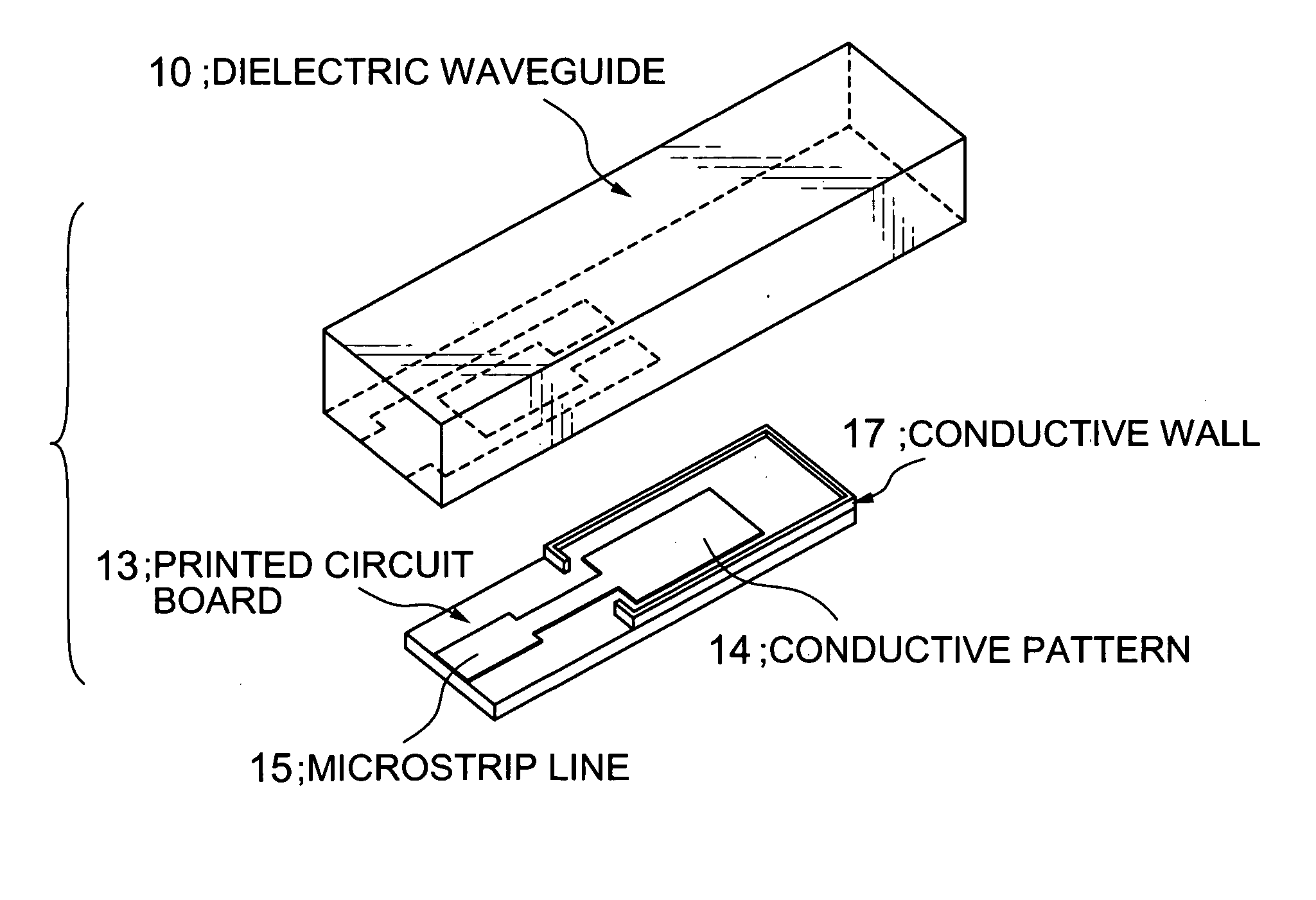
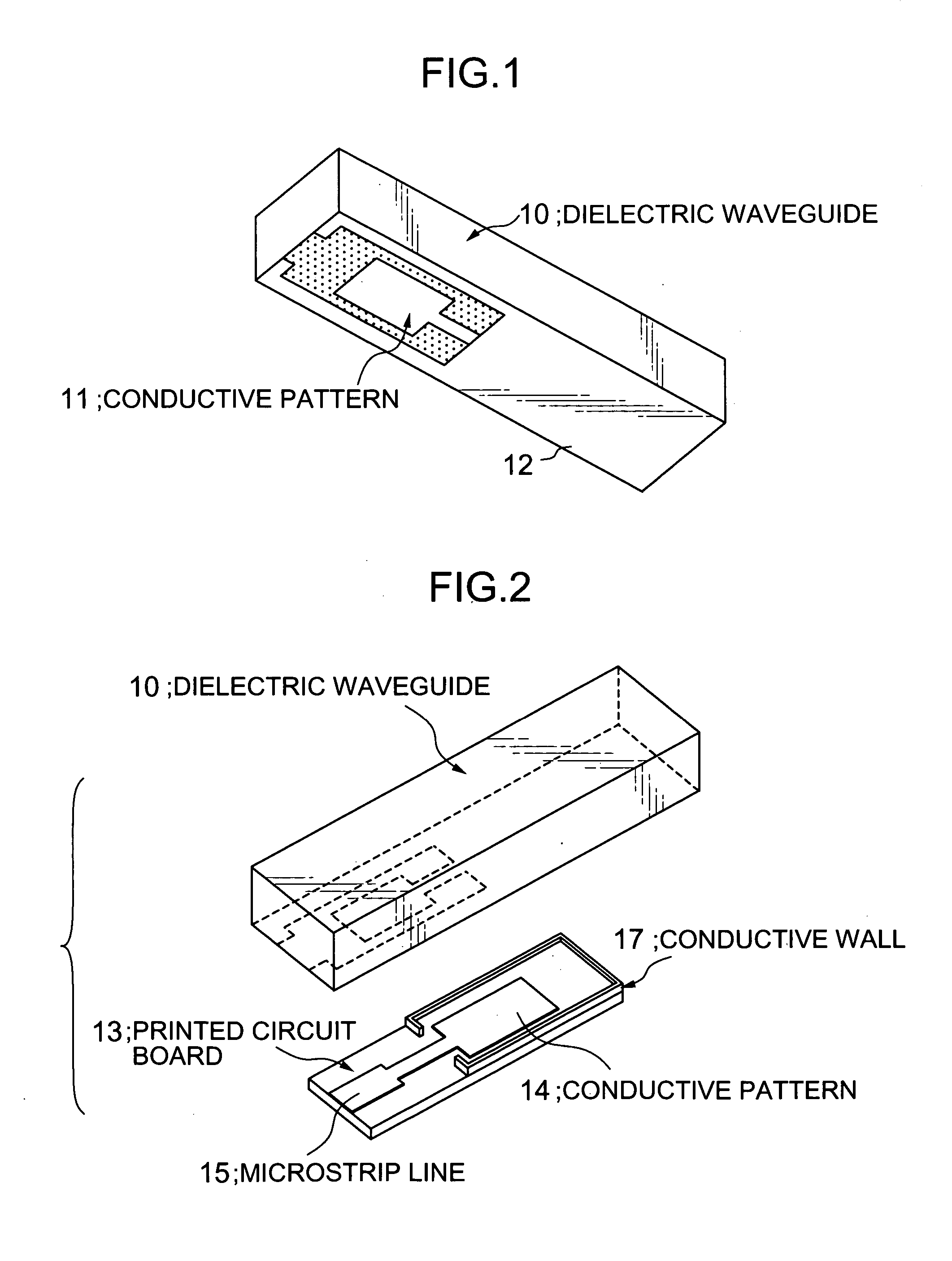
[0019] The microstrip line 15 and the dielectric waveguide 10 are electromagnetically coupled together by the opposed conductive patterns 11, 14 to allow electromagnet waves to be transmitted therebetween. In a high-frequency range, a discontinuous portion in a junction between respective transmission lines is likely to cause a large radiation loss and significant deterioration in transmission characteristics. In the coupling structure the discontinuous portion is located inside the space or cavity defined by the conductive wall, and opposed surfaces of the dielectric waveguide and the printed circuit board. Thus, the risk of the radiation of electromagnetic waves to the atmosphere can be suppressed.

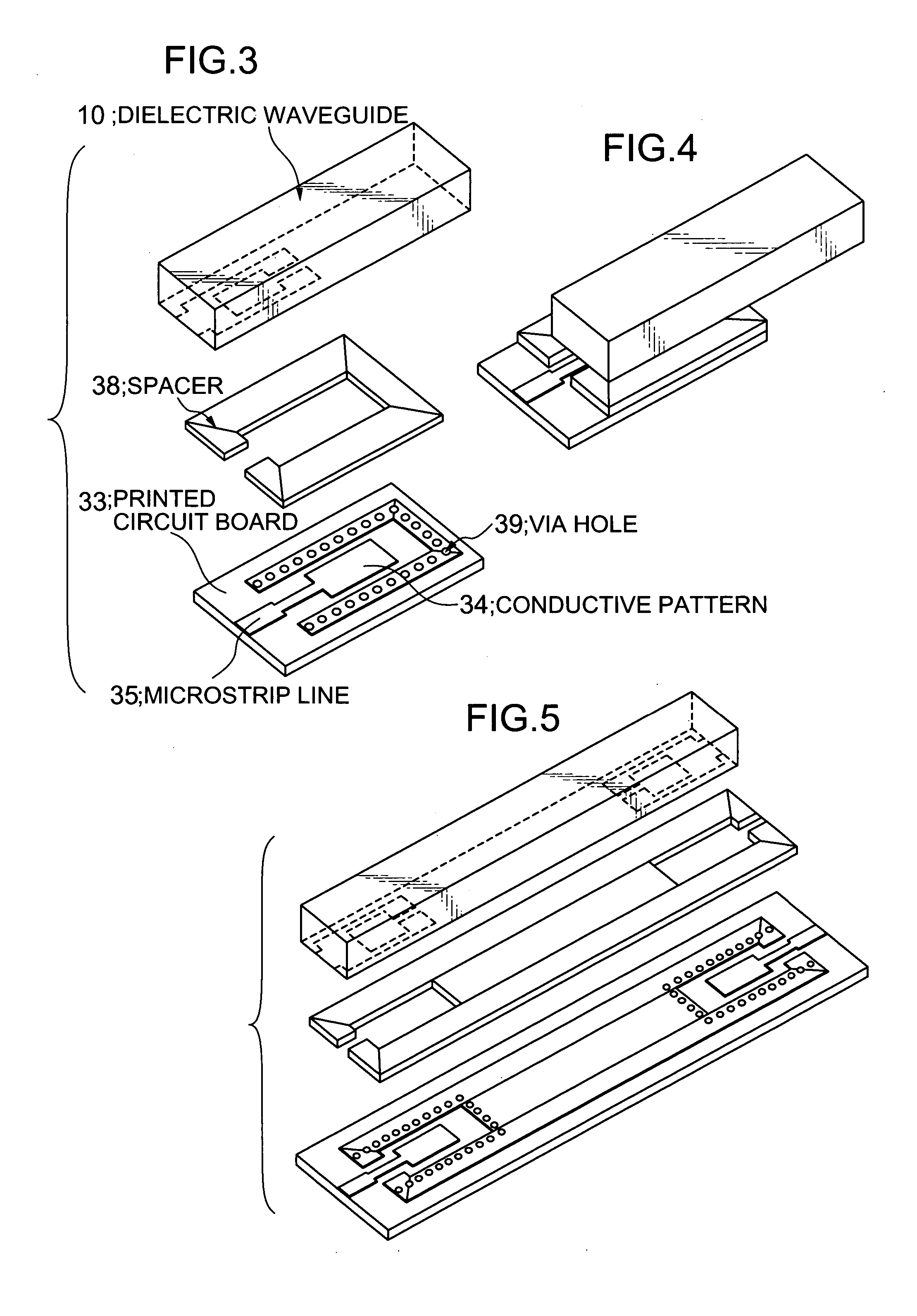
[0020]FIG. 3 shows a practical input / output coupling structure according to a second embodiment of the present invention. In this embodiment, a microstrip line 35 includes a ground conductor formed on the bottom surface of a printed circuit board 33, and a strip conductor formed on the ...

second embodiment

[0021]FIG. 5 is an exploded perspective view of a sample prepared for measuring the characteristic of the input / output coupling structure according to the present invention. The sample is formed as a filter having input and output electrodes. A dielectric waveguide with a sectional size of 4 mm×2.5 mm was prepared using a dielectric material having a specific inductive capacity of 4.5. The dielectric waveguide was designed to have a length of 30 mm, and a pair of converters was formed, respectively, at the opposite ends of the dielectric waveguide to convert between the modes in the dielectric waveguide and the microstrip line. Then, transmission and reflection characteristics were measured during the conversion. The conversion section was designed to have a length of about 7 mm. The measurement result of the conversion characteristics is shown in FIG. 6. The filter had a reflection loss of 12 dB or more, and a transmission loss of 0.6 dB in the range of 25 GHz to 29 GHz. This verif...


PUM


Abstract

Disclosed is an input/output coupling structure for coupling a printed circuit board with a dielectric waveguide having a dielectric body and a conductive film covering the dielectric body. The coupling structure comprises a first conductive pattern formed on the bottom surface of the dielectric waveguide to serve as an input/output electrode, in such a manner as to be surrounded directly by an exposed portion of the dielectric body and further by the conductive film formed around the outer periphery of the exposed portion, a spacer having a surface made substantially entirely of a conductive material and a portion for defining a given space, and a second conductive pattern formed on a principal surface of the printed circuit board and electrically connected to the microstrip line. The bottom surface of the dielectric waveguide is joined to the principal surface of the printed circuit board through the spacer, to allow the first and second conductive patterns to be located in opposed relation to one another and define the space therebetween in cooperation with the spacer. The present invention can provide a simplified structure for mounting a dielectric waveguide on a printed circuit-wiring board to couple the dielectric waveguide with a microstrip line of the dielectric waveguide, and achieve a mode conversion mechanism operable in a wide frequency band and less subject to the influence of the possible displacement between the microstrip line and the dielectric waveguide.

Description

TECHNICAL FIELD [0001] The present invention relates to a structure for coupling (connecting) a dielectric waveguide for use as resonators, filters, duplexers or the like, with a microstrip line formed on a printed circuit board. BACKGROUND ART [0002] While a cavity waveguide has been practically used as a low-loss transmission line for microwaves or millimeter waves, it involves difficulties in application to small-size electronic devices, such as portable communication terminals, due to inevitable increase in size and weight. In this connection, it is contemplated to utilize a dielectric waveguide which is prepared by forming a conductive film on a surface of a dielectric material. The dielectric waveguide has the advantage of effectively shortening the wavelength of an electromagnetic wave through its dielectric transmission line and eliminating the need for using a thick metal wall so as to facilitate downsizing and weight reduction thereof. This means that the dielectric wavegu...

Claims


Application Information

Patent Timeline
Patent Type & Authority Applications(United States)
IPC IPC(8): H01P5/103H01P5/107
CPCH01P5/107H01P3/121H01P5/103
Inventor SANO, KAZUHISA
Owner MURATA MFG CO LTD
Why Eureka
Try Eureka