Resonant converter and control method thereof

a resonant converter and control method technology, applied in the direction of electric variable regulation, process and machine control, instruments, etc., can solve the problems of troublesome circuit design, difficult design and computation of above resonant converter operating frequency, etc., to achieve reliable soft switching operation, continuous soft switching operation, and easy design

Inactive Publication Date: 2005-05-12
HITACHI LTD
View PDF2 Cites 85 Cited by
  • Summary
  • Abstract
  • Description
  • Claims
  • Application Information

AI Technical Summary

Benefits of technology

[0004] It is therefore an object of the present invention to provide a resonant converter which can realize easy design and reliable soft switching operation even in the presence of variations in characteristics between the components of a resonance circuit.
[0005] Another object of the present invention is to realize a control method of a resonant converter which can attain continuous soft switching operation even in the presence of a load variation or variations in characteristics between the components of a resonance circuit.
[0009] In accordance with the present invention, there is provided a resonant converter which can realize easy design and reliable soft switching operation even in the presence of a load variation or variations in characteristics between the components of a resonance circuit.
[0010] In the other aspect of the present invention, there is provided a control method for a resonant converter which can realize continuous soft switching operation even in the presence of a load variation or variations in characteristics between the components of a resonance circuit.

Problems solved by technology

As disclosed in Literature 1, the above resonant converter is difficult in the design and computation of an operating frequency because a load resistance varies according to an output condition.
For this reason, circuit design becomes troublesome due to the aforementioned load variation or variations in the resonance circuit components.

Method used


Image

  • Resonant converter and control method thereof
  • Resonant converter and control method thereof
  • Resonant converter and control method thereof

Examples


first embodiment

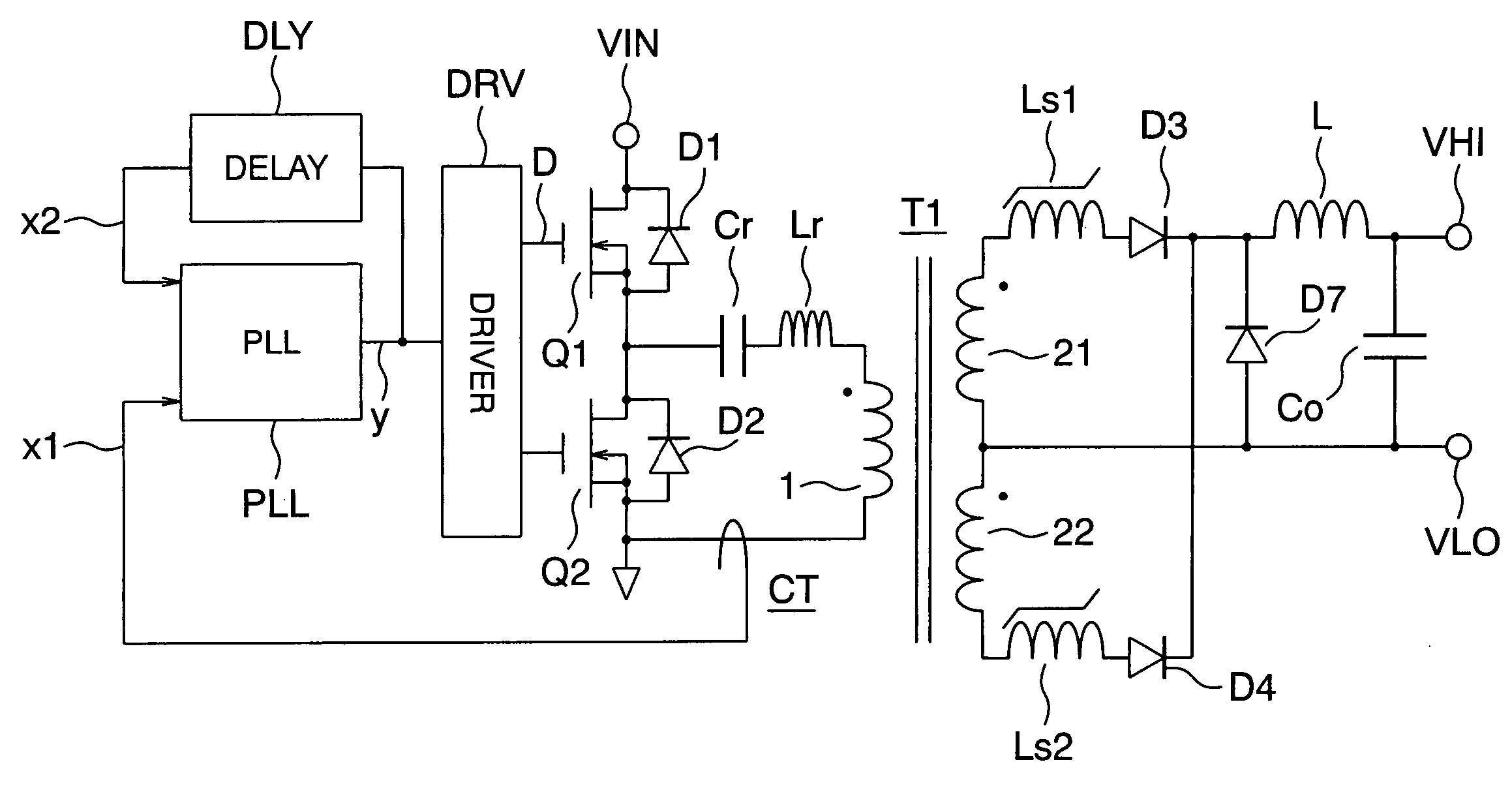
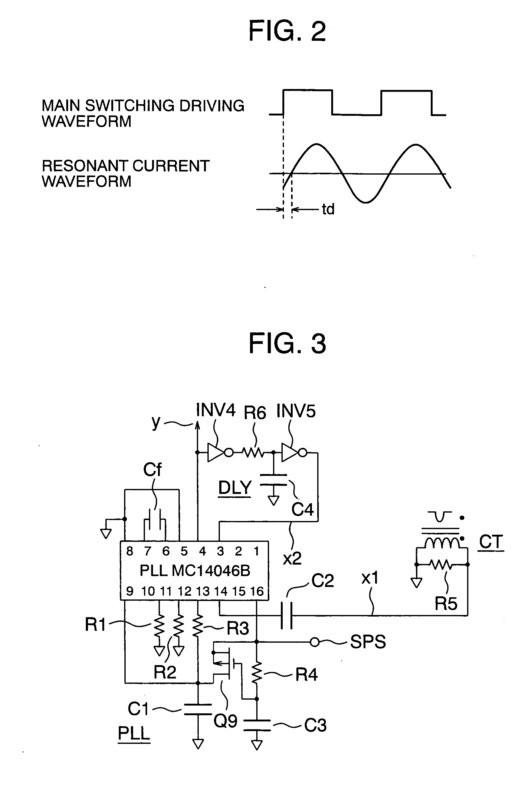
[0029]FIG. 1 is a circuit arrangement of a resonant converter in accordance with the present invention. In FIG. 1, reference symbol VIN denotes an input voltage supply terminal, symbol VHI denotes a high voltage output terminal, and VLO denotes a low voltage output terminal. A high side power MOS FET Q1 is connected to the input voltage supply terminal VIN, and a low side power MOS FET Q2 is grounded. Connected between a midpoint of the power MOS FETs Q1, Q2 and the ground voltage are an LC resonance circuit of a capacitor Cr and an inductor Lr, a primary winding 1 of a transformer T1, and the primary winding 1 of a current transformer CT, which are connected in series. An output of the current transformer CT is connected to an input line x1 as one input of a PLL (Phase Locked Loop) circuit PLL. An output line y of the PLL circuit is connected via a driver DRV to gates of the power MOS FETs Q1 and Q2, and also connected via a delay element DLY to an input line x2 of the PLL circuit ...

second embodiment

[0039]FIG. 4 is a circuit arrangement of a resonant converter in accordance with the present invention, wherein a magamp control circuit is added to the resonant converter of FIG. 1. FIG. 4 is different from FIG. 1 in that resetting diodes D5, D6, a magamp control circuit MAG, and a reference voltage Vref are added for control of the saturable reactors Ls1 and Ls2. The added circuit acts to compare the output voltage and the reference voltage Vref, and perform negative feedback control over the magamp control circuit MAG in such a manner that the output voltage is equal to the reference voltage Vref. When the output voltage is higher (lower) than the reference voltage Vref, the output voltage is fed back to the magamp control circuit MAG to decrease (increase) the output, whereby a desired output voltage can be obtained.

[0040]FIG. 5 is a specific circuit diagram of the magamp control circuit used in the embodiment of FIG. 4. The magamp control circuit MAG is composed of an error amp...

third embodiment

[0041]FIG. 6 is a circuit arrangement of a resonant converter in accordance with the present invention. The embodiment of FIG. 6 is different from that of FIG. 4 in that the diodes D3 and D4 are replaced by power MOS FETs Q3 and Q4. Since the above replacement enables the power MOS FET to have a low on-resistance, the loss can be reduced and the efficiency can be increased when compared with the use of the diodes. Diodes D31 and D41 in FIG. 6 are body diodes for the power MOS FETs Q3 and Q4. The power MOS FETs Q3 and Q4 are driven by gate driving circuit GD1 and GD2 respectively.

[0042]FIG. 7 is a specific example of a circuit arrangement of the gate driving apparatus of a power MOS FET used in the embodiment of FIG. 6. In FIG. 7, a signal extracted from a connection between the saturable reactor Ls1 or Ls2 and the transformer is used as an input to drive a transformer T2 via a level shift circuit of a capacitor C5 and two resistors R9 and R10 and via a buffer circuit BU1. And a volt...


PUM


Abstract

A resonant converter which can realize its easy design, eliminate the need for its adjustment, realize reliable soft switching operation, and increase an efficiency. A driver DRV of a main switching device uses a PLL circuit PLL to apply frequency tracking control in such a manner that a driving frequency fsw is made to track a resonant frequency fr (or 1 / N thereof, N being an odd number) and that the phase of the driving frequency fsw leads the current zero phase of the resonant frequency fr always by a desired time. As a result, such an optimum condition can be kept that the main switching device is triggered immediately before the zero-cross point of a resonant current. Thus the resonant converter which can always satisfy the optimum operational conditions, realize soft switching operation, and increase an efficiency can be realized with an easy design and a manufacturing adjustment-free arrangement.

Description

BACKGROUND OF THE INVENTION [0001] The present invention relates to an improvement in a resonant converter which converts a direct current to an alternating current as an alternating current output by a semiconductor switching device, and supplies the alternating current output to a primary side of a transformer via a resonance circuit to convert an alternating current flowing through a secondary side of the transformer into a direct current. [0002] A DC-DC converter has been widely used as an isolated power supply for the process input / output device of a computer control system or as a multioutput DC power supply for an information and communication equipment, electronic equipment and so on. One of types of such DC-DC converters is a resonant converter, which is disclosed, for example, in JP-A-2002-247854 or in “Multioutput Current-Mode Resonant Converter Using MAGAMP Control”, Switching Power Supply System Symposium 2002, Japan Management Association, (C6-2-1 to C6-2-10) (see C6-2...

Claims


Application Information

Patent Timeline
Patent Type & Authority Applications(United States)
IPC IPC(8): H02M7/21H02M3/28H02M3/335H02M3/337
CPCH02M3/33592H02M3/3376Y02B70/1475Y02B70/1433H02M2001/007Y02B70/10H02M1/0058H02M1/007H02M3/33571H02M3/015
Inventor SASE, TAKASHIKANOUDA, AKIHIKONAGAYAMA, TETSUYAHASHIMOTO, TADAHIKO
Owner HITACHI LTD
Why Eureka
Try Eureka