

Semiconductor device
a technology of semiconductor devices and impedances, applied in the direction of diodes, electronic switching, pulse techniques, etc., can solve the problems of ineffective improvement of input impedance accuracy, difficulty in forming resistances with higher accuracy, and breakage of semiconductor devices including igbts. , to achieve the effect of small temperature dependence and high accuracy
- Summary
- Abstract
- Description
- Claims
- Application Information
AI Technical Summary
Benefits of technology
Problems solved by technology
Method used
Image

Examples
embodiment 1
Preferred Embodiment 1
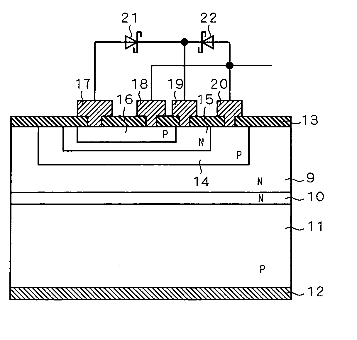
[0039]FIG. 1 is a circuit diagram illustrating a composition of a semiconductor device 5A in which an IGBT is built according to the preferred embodiment 1 of the present invention. As shown in FIG. 1, the semiconductor device 5A includes a control input terminal 1 (an input terminal), a GND terminal 2 (a reference terminal) and an output terminal 3 which are able to give and receive a signal from outside, and includes a control circuit 4, an IGBT 6, a ground resistance 7 (a first resistance) and a temperature compensation resistance 8 (a second resistance) inside.
[0040] The control circuit 4 is connected to the control input terminal 1, the GND terminal 2 and a gate electrode of the IGBT 6 and drives and controls the IGBT 6 on the basis of an input signal obtained by the control input terminal 1. A collector of the IGBT 6 is connected to the output terminal 3, and its emitter is connected to the GND terminal 2.
[0041] In the meantime, the ground resistance 7 ...
embodiment 2
Preferred Embodiment 2
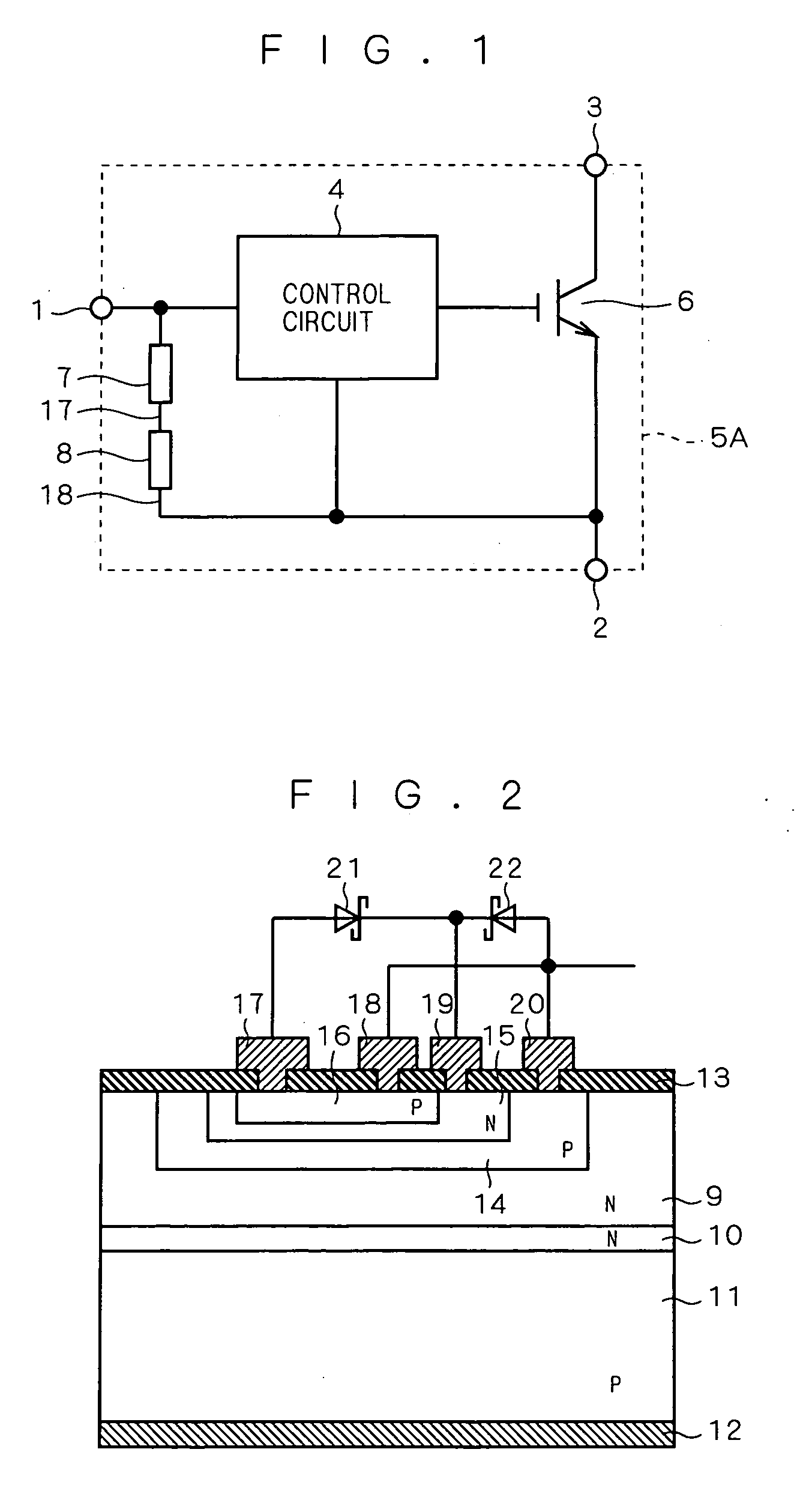
[0076]FIG. 6 is a circuit diagram illustrating a composition of a semiconductor device 5B in which an IGBT is built according to the preferred embodiment 2 of the present invention. As shown in FIG. 6, a NMOS transistor (a N type MOSFET) 23 and a schottky barrier diode 24 is interposed in parallel instead of the temperature compensation resistance 8 in the preferred embodiment 1 between the other terminal of the ground resistance 7 and the GND terminal 2. That is to say, an anode of the schottky barrier diode 24 is connected to the GND terminal 2, and its cathode is connected to the other terminal of the ground resistance 7, and moreover, a drain of the NMOS transistor 23 is connected to the other terminal of the ground resistance 7, and its source is connected to the GND terminal 2. Moreover, a gate electrode of the NMOS transistor 23 is connected directly to the control input terminal 1. Besides, other composition is similar to that of the preferred embodimen...
embodiment 3
Preferred Embodiment 3
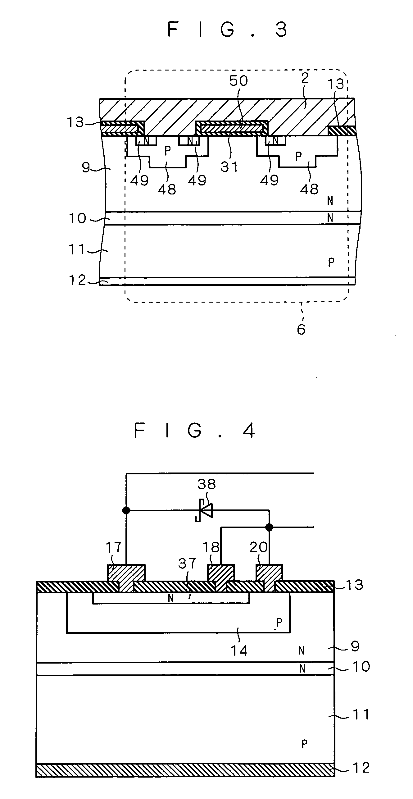
[0086]FIG. 8 is a circuit diagram illustrating a composition of a semiconductor device 5C in which an IGBT is built according to the preferred embodiment 3 of the present invention. As shown in FIG. 8, n(≧1) set(s) of (a) combined resistance part(s) RC1 to RCn is / are provided in parallel between the other terminal of the ground resistance 7 and the GND terminal 2 instead of the resistance part composed of the ground resistance 7 and the temperature compensation resistance 8 of the preferred embodiment 1.
[0087] A combined resistance part RCi (one of 1 to n is applied to i) is composed of a ground resistance RGi, a NMOS transistor QNi, a pull-up resistance RPi (a third resistance) and a zener diode TDi, one terminal of the ground resistance RGi is connected to the control input terminal 1, its other terminal is connected to a drain of the NMOS transistor QNi and a source of the NMOS transistor QNi is connected to the GND terminal 2. One terminal of the pull-up r...
PUM
 Abstract
Description
Claims
Application Information