Tape substrate and method for fabricating the same

Inactive Publication Date: 2005-05-26
LG ELECTRONICS INC +1
View PDF1 Cites 11 Cited by
  • Summary
  • Abstract
  • Description
  • Claims
  • Application Information

AI Technical Summary

Benefits of technology

[0015] The present invention has been made in view of the above mentioned problems, and an object of the invention is to provide a tape substrate and a fabricating method thereof, in which a barrier layer is formed prior to plating of tin in order to suppress formation of whiskers, thereby being capable of enhancing the quality and reliab

Problems solved by technology

As a result, a local cell is formed between the copper foil and the electroless tin plating solution, so that copper may be eluted from the copper foil pattern, thereby causing voids C to be formed at the copper foil pattern.
In severe cases, the tape substrate may be bent, thereby causing its copper foil pattern to be damaged.
Such whiskers may short-circuit adjacent pattern portions of the copper foil pattern, thereby causing circuit damage.
However, there is no method capable of effectively suppressing such whiskers.
However, the heat treatment method requires a lengthened

Method used


Image

  • Tape substrate and method for fabricating the same
  • Tape substrate and method for fabricating the same
  • Tape substrate and method for fabricating the same

Examples


example 1

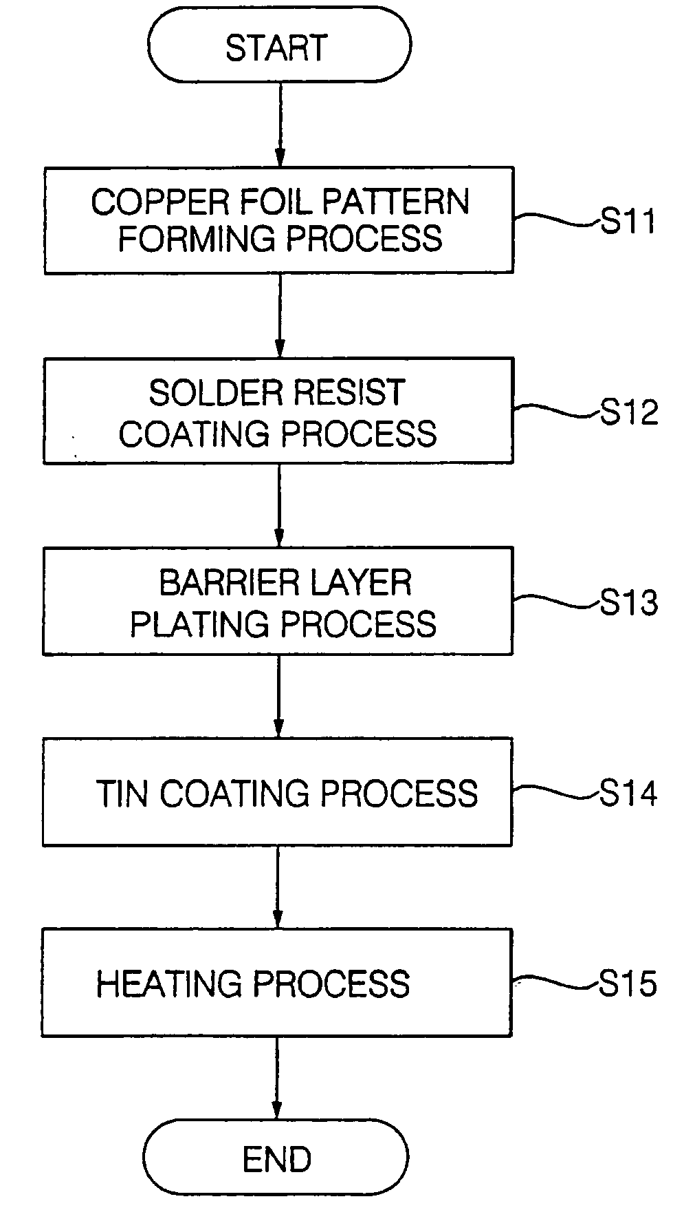
[0068] A copper foil pattern having a thickness of 18 μm was formed on a polyimide film. Thereafter, a barrier layer having a thickness of 0.1 μm was formed over the entire upper surface of the copper foil pattern. Subsequently, a solder resist was printed to a thickness of 30 μm over the barrier layer, and then thermally set at a temperature of 150° C. for 60 minutes. A tin layer was then formed over the barrier layer in a tin plating bath maintained at 65° C. In accordance with these processes, tape substrates having different tin layer thicknesses of 0.2 μm, 0.3 μm, and 0.4 μm, respectively, were fabricated. Any of the tape substrates did not exhibit voids and whiskers at the boundary of the solder resist. Even after being aged for seven days, any of the tape substrates did not exhibit whiskers even after being aged for seven days.

example 2

[0069] A copper foil pattern having a thickness of 18 μm was formed on a polyimide film. Thereafter, a solder resist was printed to a thickness of 30 μm on the upper surface of the copper foil pattern at a region other than a connecting area, and then thermally set at a temperature of 150° C. for 60 minutes. Thereafter, a barrier layer having a thickness of 0.1 μm was formed on the copper foil pattern. A tin layer was then formed over the barrier layer in a tin plating bath maintained at 65° C. In accordance with these processes, tape substrates having different tin layer thicknesses of 0.1 μm, 0.2 μm, and 0.3 μm, respectively, were fabricated. Any of the tape substrates did not exhibit voids and whiskers at the boundary of the solder resist. Even after being aged for seven days, any of the tape substrates did not exhibit whiskers.

example 3

[0070] A copper foil pattern having a thickness of 18 μm was formed on a polyimide film. Thereafter, a solder resist was printed to a thickness of 30 μm on the upper surface of the copper foil pattern at a region other than a connecting area, and then thermally set at a temperature of 150° C. for 60 minutes. Thereafter, a barrier layer having a thickness of 0.1 μm was formed on the copper foil pattern. A tin layer was then formed over the barrier layer in a tin plating bath maintained at 65° C. In accordance with these processes, tape substrates having different tin layer thicknesses of 0.2 μm, 0.3 μm, and 0.4 μm, respectively, were fabricated. After the formation thereof, the tin layer was dried at a temperature of 120° C. for 120 minutes. All tape substrates exhibited excellent characteristics.


PUM

PropertyMeasurementUnit
Thicknessaaaaaaaaaa
Stress optical coefficientaaaaaaaaaa

Abstract

A tape substrate including an insulating film, a copper foil pattern formed on the insulating film at one side of the insulating film, and provided with a connecting area where an electronic element is to be mounted, a barrier layer plated on the copper foil pattern at the connecting area, and formed with a plurality of pores, and a tin layer plated on the barrier layer, and alloyed with a portion of the copper foil pattern corresponding to the connecting area, through the pores. A method for fabricating the tape substrate is also disclosed. In accordance with the invention, it is possible to reduce the time taken for the copper foil pattern to come into contact with the electroless tin plating solution used in the tin plating process, thereby preventing the copper component of the copper foil pattern from being eluted. Accordingly, there is no open-circuit fault caused by formation of pores. The barrier layer makes it possible to obtain an improved plating efficiency and to reduce the thickness of the alloy layer. In addition, the barrier layer serves to reduce internal stress generated at the interface between the tin layer and the copper foil pattern, thereby suppressing formation of voids. Accordingly, there is an effect of preventing a short circuit caused by the growth of whiskers.

Description

[0001] This application is a Divisional of U.S. application Ser. No. 10 / 724,219 filed on Dec. 1, 2003. This Nonprovisional application claims priority under 35 U.S.C. § 119(a) on Patent Application No(s). 2002-75984 filed in KOREA on Dec. 2, 2002, the entirety of each of the above-identified documents are hereby incorporated by reference.BACKGROUND OF THE INVENTION [0002] 1. Field of the Invention [0003] The present invention relates to a tape substrate and a method for plating the tape substrate, and more particularly to a tape substrate and a fabricating method thereof, in which tin is plated on a pattern portion of the tape substrate where an electronic element is to be mounted, without formation of pores or whiskers. [0004] 2. Description of the Related Art [0005] Generally, tape substrates are mainly applicable to foldable electronic appliances such as an LCD panel, a portable phone, or a notebook computer. In pace with miniaturization and lightness of such electronic appliance...

Claims


Application Information

Patent Timeline
IPC IPC(8): B32B15/08H01L21/60C23C28/00H01L23/495H05K1/00H05K1/02H05K3/24H05K3/28
CPCH01L23/49572Y10T29/4916H05K1/0393H05K3/244H05K3/28H05K2201/0397H05K2203/1105Y10S428/901H01L2924/0002H01L23/49582Y10T428/24917Y10T428/325Y10T29/49155H01L2924/00H05K1/02B32B15/08H01L21/60
Inventor KWON, SOON BOGLEE, SANG HUNMOON, YANG SIKHONG, KI PYOCHO, YOON KUEN
Owner LG ELECTRONICS INC
Why Eureka
Try Eureka