Semiconductor device and its manufacturing method

a technology of semiconductors and manufacturing methods, applied in the direction of semiconductor devices, electrical devices, transistors, etc., can solve the problems of degrading the long-term reliability of gate insulation films, degrading the thermal stability of interfaces, etc., to reduce fabrication costs, reduce threshold voltages, and increase product yields

Active Publication Date: 2005-05-26
GK BRIDGE 1
View PDF5 Cites 79 Cited by
  • Summary
  • Abstract
  • Description
  • Claims
  • Application Information

AI Technical Summary

Benefits of technology

[0034] In accordance with the semiconductor device of the ninth aspect of the present invention, two kinds of gate electrodes of the N-type MISFET and the P-type MISFET are formed by layering films made of metal, alloy or nitride of metal. This allows the work functions of the gate electrodes to be controlled at respective optimum values by selecting the kinds and the thicknesses of the layered films. In addition, the work functions of the gate electrodes are controlled to differentiate the gate electrode of the N-type M...

Problems solved by technology

However, the above conventional technique involves the problems as shown hereinafter.
In the technique of ion-implantation of nitrogen into the Mo film, the pure metal, Mo, in direct contact with the silicon oxide film in the N-type MISFET raises the problem of degradation of the th...

Method used


Image

  • Semiconductor device and its manufacturing method
  • Semiconductor device and its manufacturing method
  • Semiconductor device and its manufacturing method

Examples


first embodiment

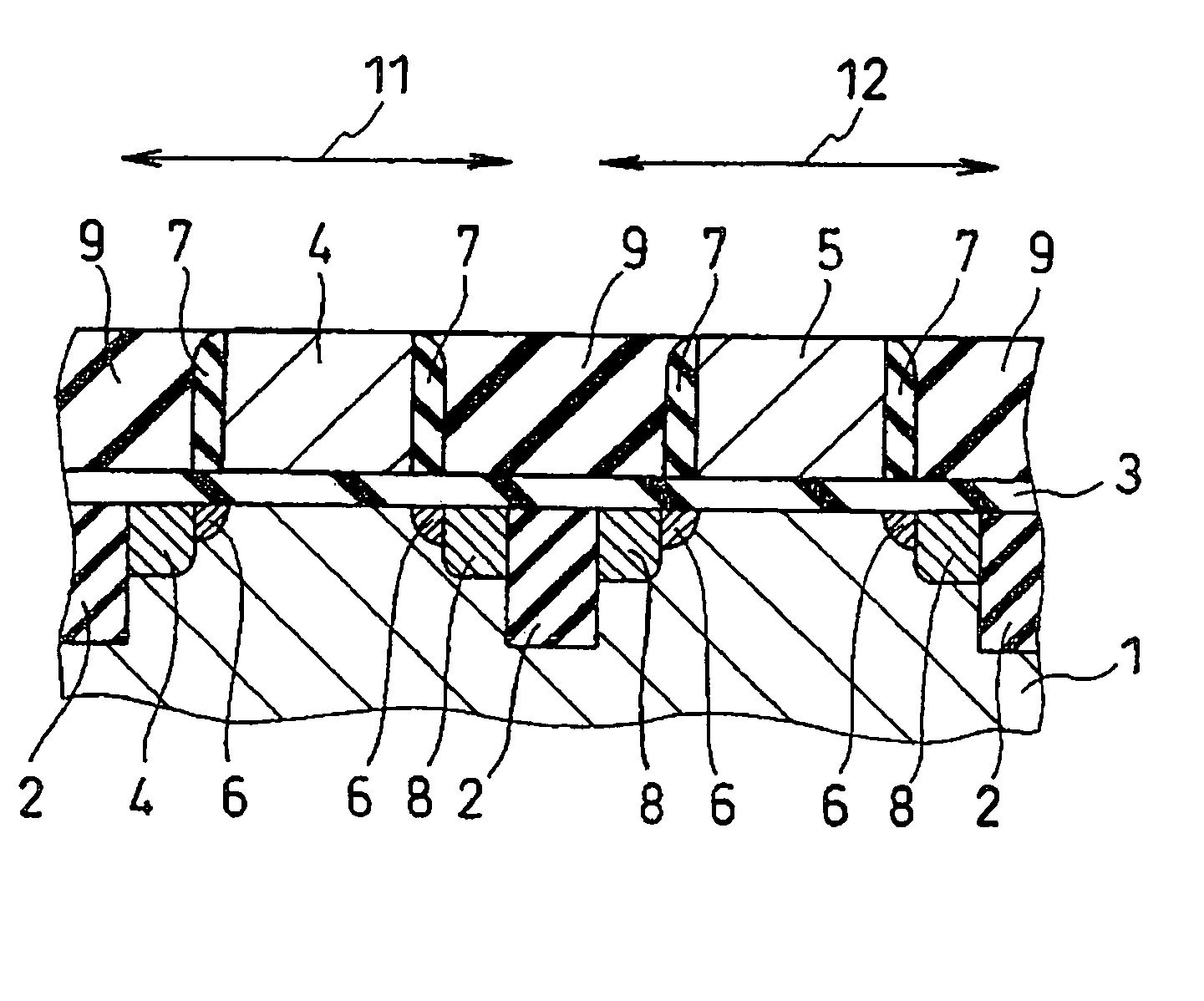
[0055] Hereinafter, embodiments of the present invention will be described more concretely with reference to accompanying drawings. For a start, the present invention will be described. FIG. 6 shows a semiconductor device according to the present embodiment. As shown in FIG. 6, in the semiconductor device of the present embodiment, a silicon substrate 1 is provided, and element isolation regions 2 are selectively formed in the surface area of the silicon substrate 1. An insulation film, such as made of SiO2, is received in the element isolation region 2, and the space between the element isolation regions 2 constitutes an N-type MISFET forming region 11 or a P-type MISFET forming region 12. The depth of the element isolation region 2 is 100 to 500 nm, for example, whereas the distance between the element isolation regions is 0.05 to 10 μm, for example.

[0056] In each of the N-type MISFET forming region 11 and P-type MISFET forming region 12 in the surface area of the silicon substrat...

second embodiment

[0097] If there is a high-temperature process at a temperature equal to or above 400 degrees C. after formation of the gate electrodes, and a pure metal is used as a film underlying the metal gates, then there will be a reaction in the interface between the pure metal film and the gate insulation film (for example, silicon oxide film) in the high-temperature process, thereby deviating the threshold from the design value. Thus, it is preferable to select a metal nitride film having a higher thermal stability as the film underlying the metal gate. However, it is possible to form dummy gate insulation film and dummy gate electrode, followed by ion-implantation and activation of impurities, removal of the dummy gate insulation film and dummy gate electrode and formation of the gate insulation film and gate electrode in the present embodiment, as in the This allows a material having a relatively lower resistance against heat can be used as the gate electrode material. For example, a HfN...


PUM


Abstract

A method for manufacturing a semiconductor device wherein both the threshold voltages of an N-type MISFET and a P-type MISFET are low, device can be easily manufactured at a lower cost and a higher product yield, and the reliability of the gate insulation film is higher. The gate insulation film is formed on the surface of a silicon substrate 1 in N-type MISFET forming region and the P-type MISFET forming region, and metal gates 4 and 5 are provided thereon. The metal gate 4 is made from a TiCoN film, and the work function thereof is set at 4.0 to 4.8 eV suited to the gate electrode material of the N-type MISFET. The metal gate 5 is formed from a portion of the TiCoN film by ion-implantation of oxygen into the TiCoN film configuring the gate electrode 4 at a dosage of 1013 to 1014 (ions/cm2) to raise the work function by around 0.2 to 0.8 eV.

Description

FIELD OF THE INVENTION [0001] The present invention relates to a semiconductor device and a method for manufacturing the same, and more particularly, to a semiconductor device, which includes an N-channel metal-insulator-semiconductor field-effect transistor (MISFET) and a p-channel MISFET both having metal gates and is capable of reducing a threshold voltage of each of the FETs to realize a higher operational speed. BACKGROUND TECHNOLOGY [0002] For increasing the integration density as well as improving the performances of semiconductor devices, development of finer structures has been achieved for the MISFETs constituting the semiconductor device. However, since the finer structure of the MISFET increases the influence by the short-channel effect thereof, it is an important subject to reduce the short-channel effect. Among other proposals for the suppression of the short-channel effect based on the technique in accordance with a so-called scaling rule, a proposal uses a reduced th...

Claims


Application Information

Patent Timeline
IPC IPC(8): H01L29/423H01L21/336H01L21/8234H01L21/8238H01L27/092H01L29/49H01L29/78
CPCH01L21/823437H01L21/823857H01L21/823828H01L21/823462
Inventor YOSHIHARA, TAKUYA
Owner GK BRIDGE 1
Why Eureka
Try Eureka