Advanced process control approach for Cu interconnect wiring sheet resistance control

a technology of process control and wiring sheet, applied in adaptive control, lapping machines, instruments, etc., can solve the problems of unprofitable fabrication methods, no manufacturing approach to control copper rs variations, and no known algorithm that can be applied to a cmp process to control copper sheet resistance, etc., to achieve the effect of minimizing cu sheet resistance (rs) variations in copper interconnects

Inactive Publication Date: 2005-05-26
TAIWAN SEMICON MFG CO LTD
View PDF11 Cites 40 Cited by
  • Summary
  • Abstract
  • Description
  • Claims
  • Application Information

AI Technical Summary

Benefits of technology

[0012] An objective of the present invention is to provide an APC method for a CMP process that minimizes Cu sheet resistance (Rs) variations in copper interconnects.
[0015] Yet another objective of the present invention is to provide a wafer based Cu CMP APC method that reduces Cu Rs variations for a variety of wiring pattern densities.

Problems solved by technology

Currently, there is no manufacturing approach to control copper Rs variations.
Still, there is no known algorithm that can be applied to a CMP process to control copper sheet resistance.
However, monitor wafers may be over utilized to the extent that the fabrication method becomes unprofitable because of the loss of production time or down time associated with monitors.

Method used


Image

  • Advanced process control approach for Cu interconnect wiring sheet resistance control
  • Advanced process control approach for Cu interconnect wiring sheet resistance control
  • Advanced process control approach for Cu interconnect wiring sheet resistance control

Examples


Embodiment Construction

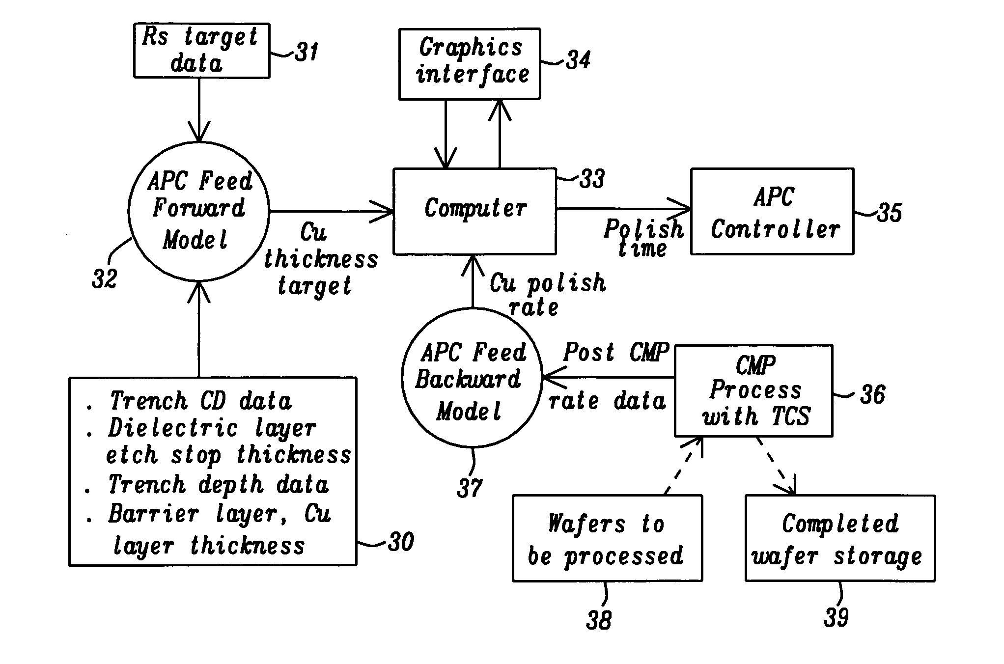
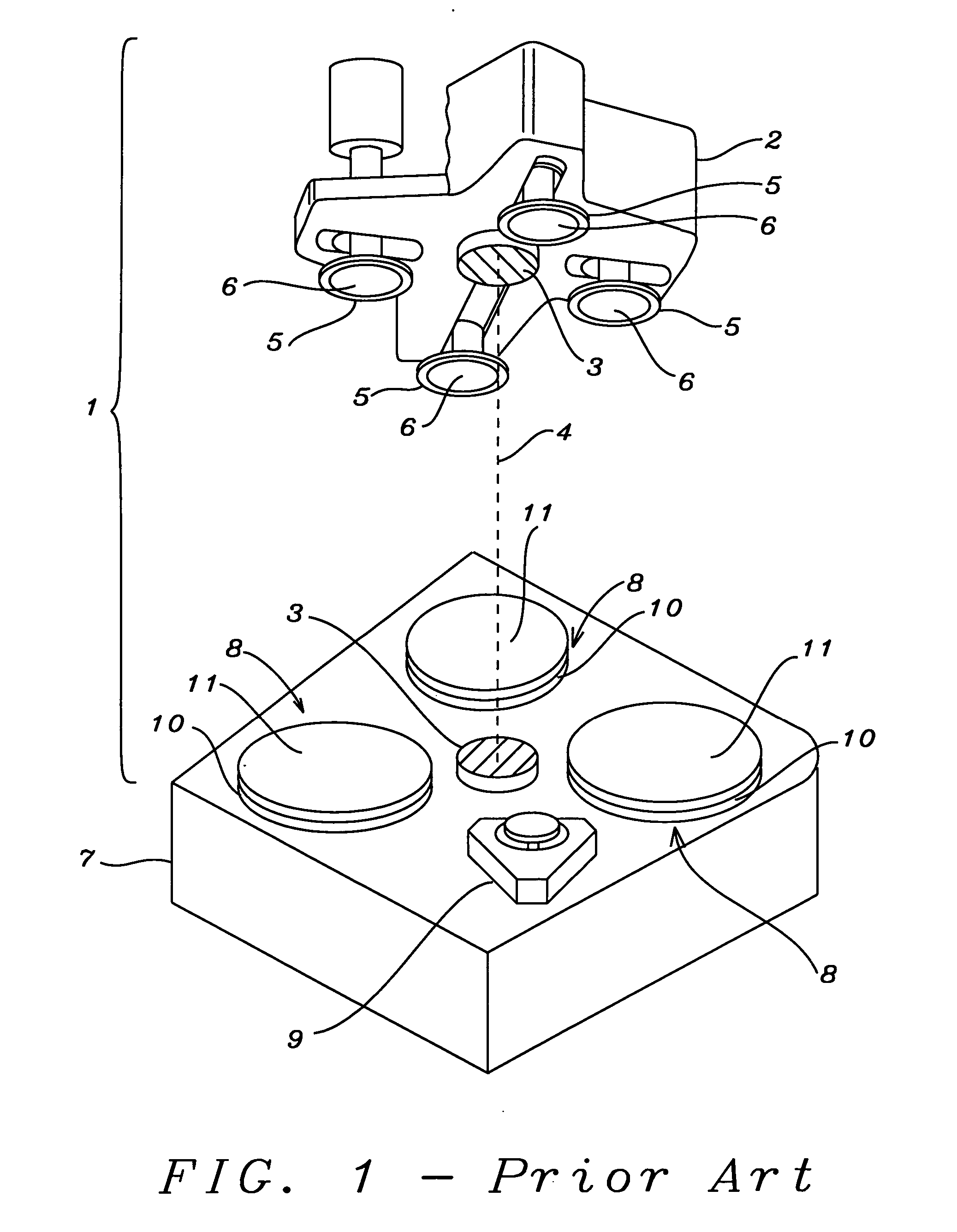
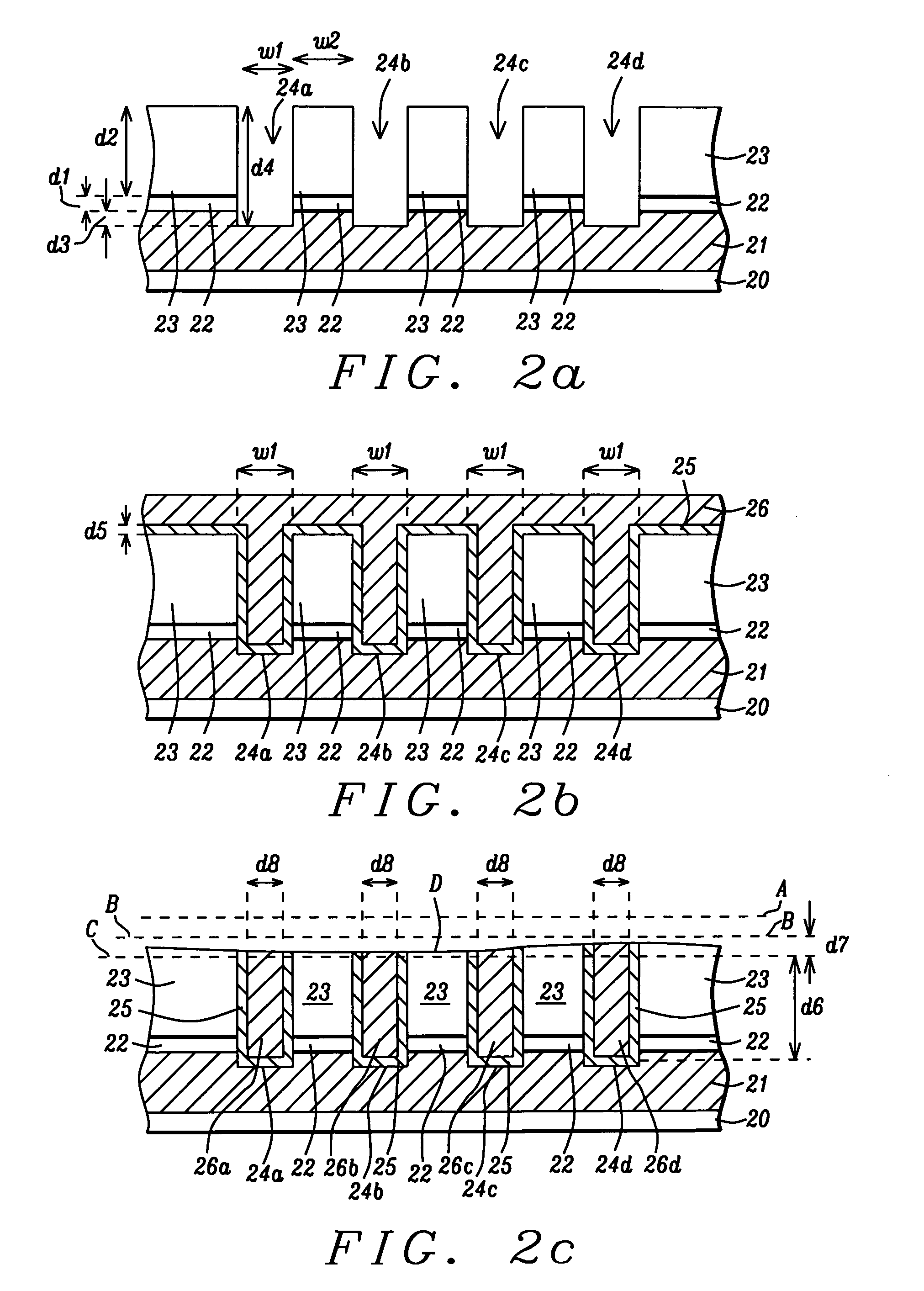
[0027] The present invention is an advanced process control (APC) method that is particularly useful for minimizing copper sheet resistance (Rs) in copper interconnects formed in a semiconductor device. Although a single damascene structure involving a trench formed in a dielectric layer on a substrate is shown in the drawings, other types of copper interconnects such as those comprising a trench and a via in a dual damascene scheme or stacked layers of metal wiring that are fabricated by performing a plurality of damascene processes are also within the scope of this invention. Furthermore, the APC method for controlling an oxide (Cu, TaN) polish step is not necessarily limited to only copper interconnects but may be applied to the fabrication of interconnects comprised of other metals such as Al / Cu alloys, Al, and W which are formed in a dielectric layer. Moreover, other diffusion barrier layers such as TiN, Ta / TaN, or Ti / TiN may be used in place the TaN layer in the exemplary embo...


PUM

PropertyMeasurementUnit
thickness d1aaaaaaaaaa
temperaturesaaaaaaaaaa
thickness d2aaaaaaaaaa

Abstract

A wafer based APC method for controlling an oxide (Cu, or TaN) polish step is described and combines a feed forward model that compensates for incoming wafer variations with a feed backward model which compensates for CMP variations. The method is geared toward minimizing Rs 3σ variations. A Rs target value is inputted with metrology data from previous processes that affects the width and thickness of the copper layer. A copper thickness target and polish time for the first wafer is determined. Post CMP measurement data of the first wafer is used to modify the polish rate with a disturbance factor and an updated polish time is computed for subsequent wafers. The CMP recipe for each wafer is adjusted with metrology data and post CMP measurements. The APC method is successful in controlling copper Rs variations for the 90 nm technology node and is independent of copper pattern density.

Description

RELATED PATENT APPLICATION [0001] This application is related to the following: Docket # TSMC02-1068, Ser. No. ______ filing date ______; assigned to a common assignee.FIELD OF THE INVENTION [0002] The invention relates to the field of fabricating integrated circuits and in particular to a method of performing a chemical mechanical polishing step on copper wiring with a higher degree of process control to enable copper sheet resistance to be minimized. BACKGROUND OF THE INVENTION [0003] The use of copper wiring as interconnects in semiconductor devices has increased dramatically as ground rules shrink in order to prevent capacitance coupling or crosstalk between metal lines. Interconnects are typically formed by a damascene approach in which a metal layer is deposited in an opening etched into one or more dielectric layers on a substrate. An important aspect of the damascene process is planarization of the metal layer which becomes coplanar with the top dielectric layer. A chemical ...

Claims


Application Information

Patent Timeline
Patent Type & Authority Applications(United States)
IPC IPC(8): B24B37/04B24B51/00G05B13/02H01L21/3105H01L21/321
CPCB24B37/042B24B51/00H01L21/3212H01L21/31053G05B13/024
Inventor LIN, CHUN HSIENLIU, AI-SENWU, SUNNYLIN, YU-LIANGLO, HENRYZHOU, MEI-SHENG
Owner TAIWAN SEMICON MFG CO LTD
Why Eureka
Try Eureka