Semiconductor device
- Summary
- Abstract
- Description
- Claims
- Application Information
AI Technical Summary
Benefits of technology
Problems solved by technology
Method used
Image

Examples
first embodiment
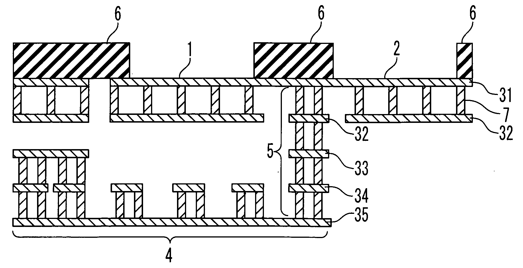
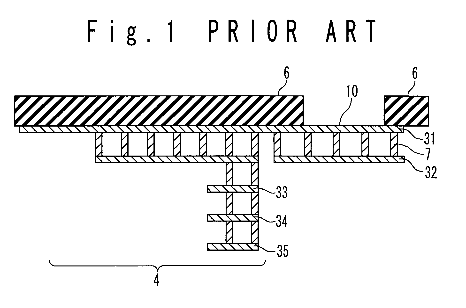
[0043]FIG. 6 is a top view showing a semiconductor chip 100 of a semiconductor device according to the first embodiment of the present invention. As shown in FIG. 6, the semiconductor device has a plurality of bonding pads 1 and a plurality of test pads 2. The “bonding pad 1” is used for a bonding and is configured to be bonded to a bonding member. The “test pad 2” is used for a testing and is configured to contact with a test probe at the testing. The plurality of test pads 2 are provided for respective of the plurality of bonding pads 1. As shown in FIG. 6, the plurality of bonding pads 1 and the plurality of test pads 2 are formed on a peripheral region of the semiconductor chip 100. Here, on the semiconductor chip 100, a region where the plurality of test pads 2 are formed is outer than a region where the plurality of bonding pads 1 are formed. That is to say, each test pad 2 is located between corresponding one bonding pad 1 and an edge of the semiconductor chip 100.
[0044] Als...
second embodiment
[0060] A semiconductor device according to the second embodiment is different from that of the first embodiment in that the internal circuit 4 is formed not only under the bonding pad 1 but also under the test pad 2. That is to say, the test pad 2 is also formed to overlap with the internal circuit 4. Here, the internal circuit 4 under the test pad 2 is provided sufficiently away from the test pad 2. More specifically, the internal circuit 4 formed under the test pad 2 is located lower than the internal circuit 4 formed under the bonding pad 1. The detailed configuration will be described below in detail.
[0061] As in the first embodiment, the bonding pad 1 and the test pad 2 in the present embodiment are formed on the peripheral region of the semiconductor chip 100 (see FIG. 6). Moreover, the test pad 2 is located between the bonding pad 1 and an edge of the semiconductor chip 100.
[0062]FIG. 10 is a cross sectional view showing around the bonding pad 1 and the test pad 2 of the se...
PUM
 Abstract
Description
Claims
Application Information
 - Generate Ideas
- Intellectual Property
- Life Sciences
- Materials
- Tech Scout
- Unparalleled Data Quality
- Higher Quality Content
- 60% Fewer Hallucinations
Browse by: Latest US Patents, China's latest patents, Technical Efficacy Thesaurus, Application Domain, Technology Topic, Popular Technical Reports.
© 2025 PatSnap. All rights reserved.Legal|Privacy policy|Modern Slavery Act Transparency Statement|Sitemap|About US| Contact US: help@patsnap.com