
Method of forming high voltage metal oxide semiconductor transistor

a metal oxide semiconductor and high-voltage technology, applied in the direction of transistors, semiconductor devices, electrical appliances, etc., can solve the problems of affecting the doping effect of the transistor, and achieve the effect of improving the breakdown voltag

Active Publication Date: 2005-06-02
UNITED MICROELECTRONICS CORP
View PDF8 Cites 28 Cited by
  • Summary
  • Abstract
  • Description
  • Claims
  • Application Information

AI Technical Summary

Benefits of technology

[0010] It is therefore a primary object of the claimed invention to provide a method of forming a HVMOS transistor for improving the breakdown voltage.
[0012] It is an advantage of the claimed invention that the photoresist layer originally used to form the gate is used as a hard mask to perform two ion implantation processes such that the doped regions are deeper than the doped regions of the prior art. Hence, the breakdown voltage is effectively improved.

Problems solved by technology

However, the thickness of the gate 26 hinders the doped energy during the ion implantation processes.

Method used


Image

  • Method of forming high voltage metal oxide semiconductor transistor
  • Method of forming high voltage metal oxide semiconductor transistor
  • Method of forming high voltage metal oxide semiconductor transistor

Examples


Embodiment Construction

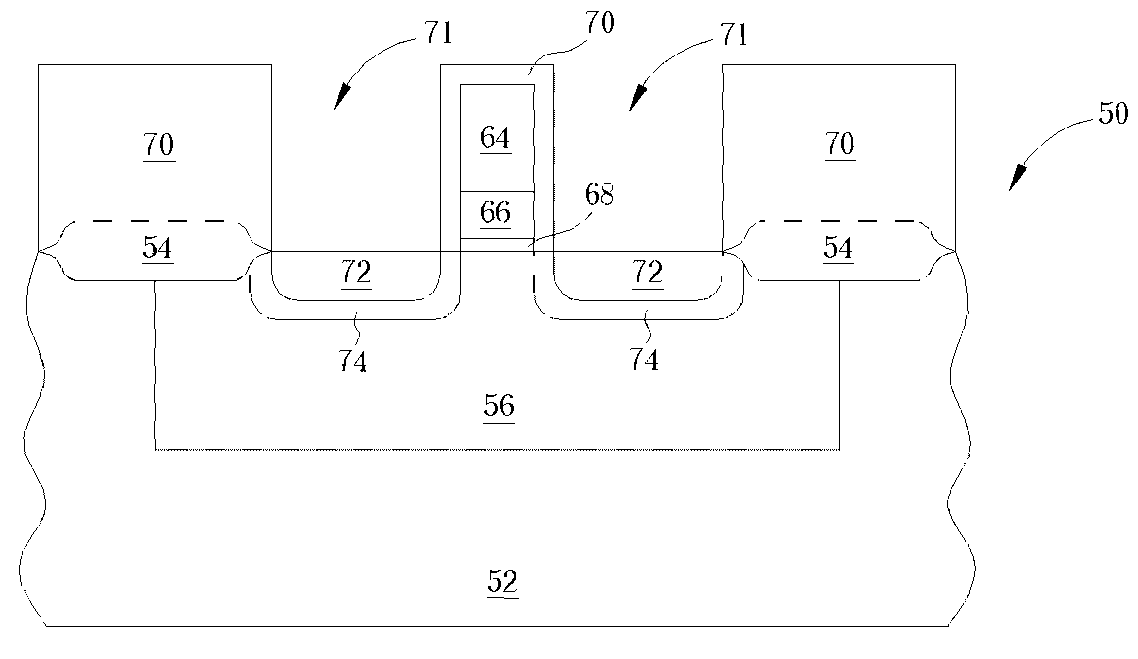
[0018] Please refer to FIG. 6 to FIG. 10. FIG. 6 to FIG. 10 are schematic diagrams illustrating a method of forming a P type HVMOS transistor 50 with DDD according to a preferred embodiment of the present invention. As shown in FIG. 6, first a substrate 52 is provided. The substrate 50 can be a polysilicon substrate, an epitaxial silicon substrate, or a silicon on insulator (SOI) substrate. Then, a thermal oxidation process is carried out to form two field oxide layers 54 in the substrate 52, and an N type well is formed in the substrate 52 by doping ions, such as phosphorous (P) or arsenic (As), into the substrate 52 between the field oxide layers 54. The field oxide layers 54 are for insulating adjacent HVMOS transistors or other components, and thus other structures such as trenches can replace the field oxide layers 54 in the present invention.

[0019] As shown in FIG. 7, a thermal oxidation process is carried out to form an oxide layer 58 on the substrate 52, and then a polysili...


PUM


Abstract

A polysilicon layer and a first patterned photoresist layer are formed on a substrate. An ultraviolet curing process is performed to cure the first patterned photoresist layer. Then, a gate structure is formed by using the first patterned photoresist layer as a hard mask. A second patterned photoresist layer is formed on the substrate. The second patterned photoresist layer, the cured remaining first patterned photoresist layer and the gate form two openings alongside the gate structure. Finally, via the openings, two consecutive ion implantation processes are performed to form a double diffuse drain (DDD) structure.

Description

BACKGROUND OF INVENTION [0001] 1. Field of the Invention [0002] The present invention relates to a method of forming a high voltage metal oxide semiconductor (HVMOS) transistor, and more particularly, to a method of forming a HVMOS transistor with a double diffuse drain (DDD). [0003] 2. Description of the Prior Art [0004] Double diffuse drain (DDD) is a source / drain structure that is applied to HVMOS transistors. The DDD structure is able to provide the HVMOS transistor with a higher breakdown voltage. This can prevent a high voltage, such as electrostatic discharge (ESD), from damaging the transistor. Furthermore, the hot electron effect resulting from short channel is avoided. [0005] Please refer to FIG. 1 showing a schematic diagram of a conventional HVMOS transistor 10 with DDD. As shown in FIG. 1, the HVMOS transistor 10 is formed in a substrate 12. The substrate 12 comprises two field oxide layers 14 formed in the substrate 12, a first conductive type well 16 formed in the sub...

Claims


Application Information

Patent Timeline
Patent Type & Authority Applications(United States)
IPC IPC(8): H01L21/266H01L21/336H01L29/78
CPCH01L21/266H01L29/7833H01L29/6659
Inventor CHEN, CHIN-LONG
Owner UNITED MICROELECTRONICS CORP
Features
  • Generate Ideas
  • Intellectual Property
  • Life Sciences
  • Materials
  • Tech Scout
  • Unparalleled Data Quality
  • Higher Quality Content
  • 60% Fewer Hallucinations
Learn More