Method for fabricating trench capacitors for integrated semiconductor memories

a semiconductor memory and trench capacitor technology, applied in the direction of semiconductor devices, electrical equipment, transistors, etc., can solve the problems of enlargement of the surface of the trench capacitor, and achieve the effects of preventing the constriction of the upper trench region, good covering, and sufficient protection

Inactive Publication Date: 2005-06-02
POLARIS INNOVATIONS LTD
View PDF6 Cites 18 Cited by
  • Summary
  • Abstract
  • Description
  • Claims
  • Application Information

AI Technical Summary

Benefits of technology

[0074] The opening method makes it possible to etch the semiconductor substrate in a well-defined region within the upper trench region, namely between the first etching-back step and the second etching-back step.
[0075] The insulator (“buried collar”) is preferably produced on the zone etched in the upper trench region, preferably between the first etching-back step and the second etching-back step. This configuration of the insulator counteracts constriction of the upper trench regions. Furthermore, the etching in the upper trench region makes it possible, without trench constriction, to produce an insulator with such a large layer thickness in the upper trench region that the threshold voltage of the parasitic transistor at the upper trench region is put so high that no parasitic transistor currents can discharge the storage capacitor.
[0076] In a preferred embodiment, the second liner is applied to the dielectric. As a result, the dielectric need not be removed before the production of the buried collars. At the same time, the dielectric and the second liner together form, e.g. in the form of an NO layer, a good covering during the etching of the semiconductor substrate in the upper trench region.
[0077] In another preferred embodiment, the second liner is applied to the semiconductor substrate. In this case, it is necessary to remove the dielectric before the application of the second liner at least in the open regions. However, a later step for removing the dielectric is obviated. Given a sufficient thickness, the second liner affords, also as a single layer, sufficient protection during the selective etching of the semiconductor substrate in the upper trench region.

Problems solved by technology

Furthermore, it is possible to carry out etching steps that roughen the surfaces of the trench walls in the lower trench region, which leads to an enlargement of the surface of the trench capacitors.

Method used


Image

  • Method for fabricating trench capacitors for integrated semiconductor memories
  • Method for fabricating trench capacitors for integrated semiconductor memories
  • Method for fabricating trench capacitors for integrated semiconductor memories

Examples


Embodiment Construction

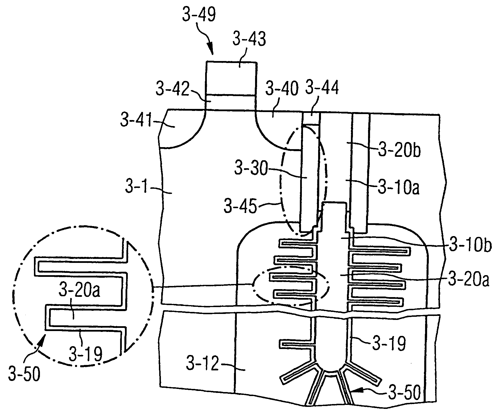
[0089] Referring now to the figures of the drawing in detail and first, particularly, to FIGS. 3A-3H thereof, there is shown an embodiment of a method according to the invention for fabricating memory cells with trench capacitors and selection transistor.

[0090]FIG. 3A shows a semiconductor substrate 3-1, which is a p-doped silicon wafer in this embodiment, with an applied layer stack containing a thin pad oxide 3-2, a nitride layer 3-3, an oxide 3-4 having a thickness of about 1 μm to 2 μm, and a polysilicon layer 3-5 having a thickness of 200 nm to 300 nm. A TEOS layer 3-4 may also contain other oxides, e.g. silane oxide.

[0091] Afterwards, the polysilicon layer 3-5 is patterned with the aid of a standard photolithographic method that prescribes the structure, position and cross section of the trenches to be produced for the trench capacitors in the semiconductor substrate 3-1. Afterwards, a first horizontal mask 3-8a is produced selectively with respect to the polysilicon layer 3...


PUM


Abstract

In a method for fabricating trench capacitors, in particular for memory cells having at least one selection transistor for integrated semiconductor memories, a trench for the trench capacitor is formed. The trench has a lower trench region, in which the capacitor is disposed, and an upper trench region, in which an electrically conductive connection from an electrode of the capacitor to a diffusion zone of the selection transistor is disposed. The method reduces the number of process steps for the fabrication of memory cells and enables fabrication of buried collars in the storage capacitors with an insulation quality as required for the fabrication of very large-scale integrated memory cells (<300 nm trench diameter).

Description

CROSS-REFERENCE TO RELATED APPLICATION [0001] This application is a continuation of copending International Application No. PCT / EP02 / 00102, filed Jan. 8, 2002, which designated the United States and was not published in English.BACKGROUND OF THE INVENTION [0002] Field of the Invention [0003] The invention relates to a method for fabricating trench capacitors for integrated semiconductor memories. [0004] The advancing miniaturization of circuits of semiconductor components leads to the demand for capacitors with the largest possible capacitance-to-volume ratio. Large-scale integrated semiconductor memories, in particular, require, for charge storage purposes, capacitors which have to provide a capacitance of at least about 30 fF in conjunction with a very small area requirement. [0005] In addition to thinning the dielectric layer between the two capacitor electrodes and increasing the dielectric constant through the choice of new materials, in particular enlarging the surfaces of the...

Claims


Application Information

Patent Timeline
Patent Type & Authority Applications(United States)
IPC IPC(8): H01L21/20H01L21/8242H01L27/108
CPCH01L27/1087H01L27/10867H10B12/0385H10B12/0387H10B99/00
Inventor GOLDBACH, MATTHIASLUTZEN, JORNORTH, ANDREAS
Owner POLARIS INNOVATIONS LTD
Why Eureka
Try Eureka