Timing closure methodology

a timing closure and timing technology, applied in the direction of cad circuit design, program control, instruments, etc., can solve the problems of difficult to compare two circuits for performance advantages, routing completion is not guaranteed to be achieved, and the excess timing in one module cannot generally be compensated by another module, so as to facilitate the maintenance of timing closure and avoid costly timing analysis

Inactive Publication Date: 2005-06-02
IBM CORP +1
View PDF52 Cites 19 Cited by
  • Summary
  • Abstract
  • Description
  • Claims
  • Application Information

AI Technical Summary

Benefits of technology

[0026] The present invention makes possible an advantage of facilitating the maintenance of timing closure throughout the design process. The invention makes possible another advantage of compensating for the unpredictable delay effects due to the placement and routing steps in the design process.
[0027] Still another advantage made possible by the invention is the avoidance of costly timing analysis of conventional approaches. In contrast, timing analysis is required during placement and throughout the conventional design process.

Problems solved by technology

In contrast, excess timing in one module cannot generally be compensated by another module.
In contrast, it is difficult to compare two circuits for performance advantages, based on timing, since timing may be different for every circuit path.
Third, if circuit area is established as a constraint, then routing completion is not guaranteed to be achieved.

Method used


Image

  • Timing closure methodology
  • Timing closure methodology
  • Timing closure methodology

Examples


Embodiment Construction

[0050] Those of ordinary skill in the art will realize that the following description of the present invention is illustrative only and not in any way limiting. Other embodiments of the invention will readily suggest themselves to those skilled in the art.

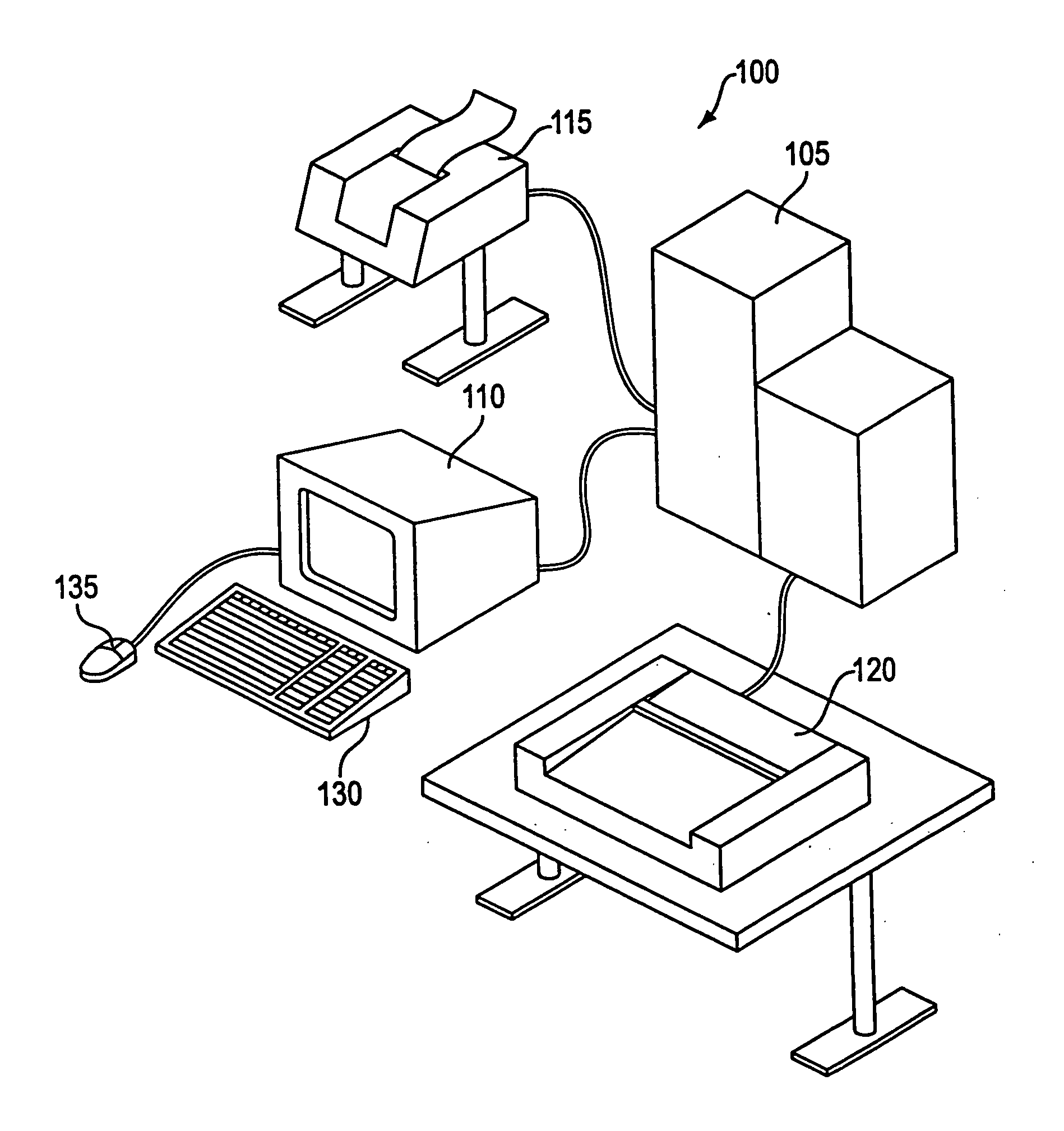
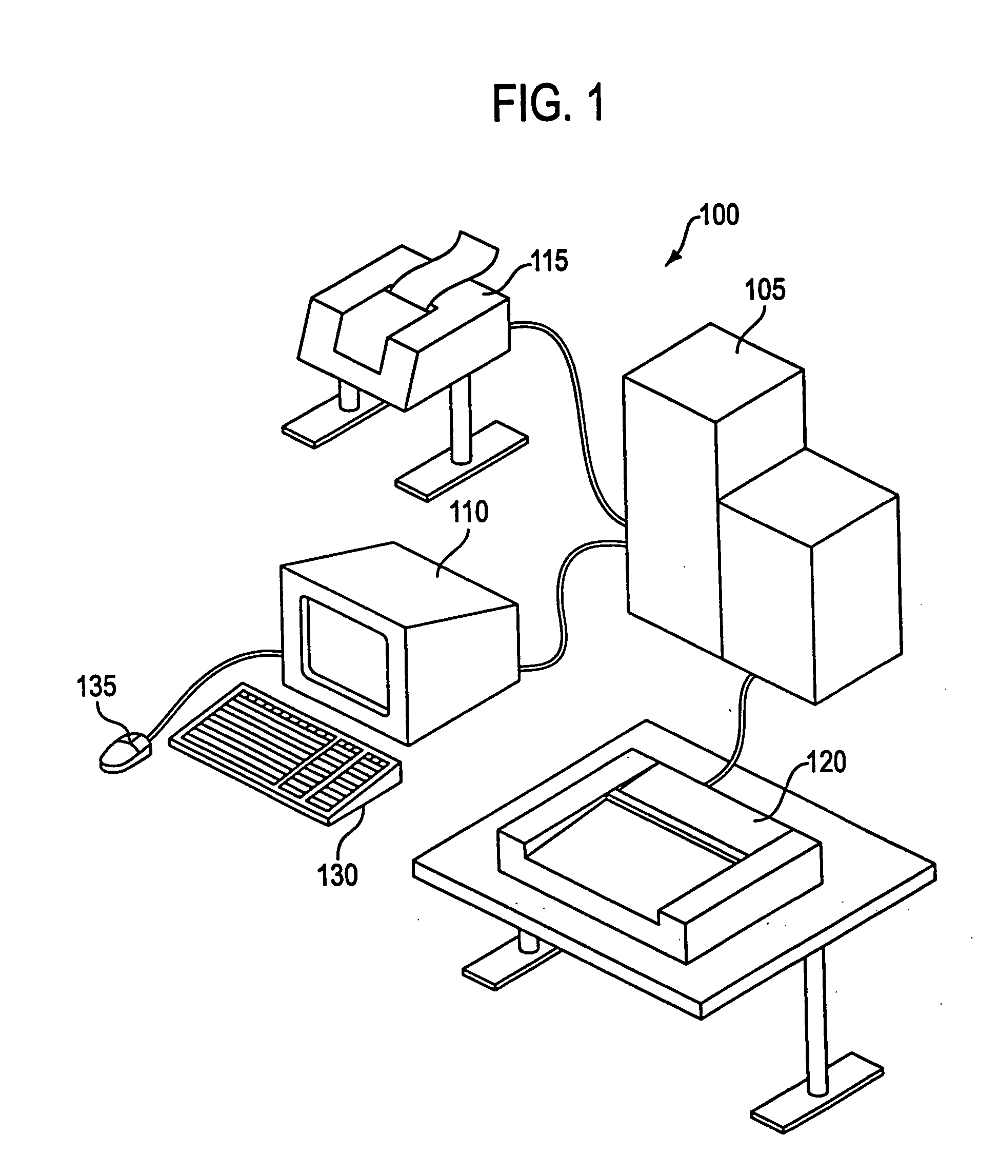
[0051] Referring in detail now to the drawings wherein similar parts or steps of the present invention are identified by like reference numerals, there is seen in FIG. 1 a schematic diagram of a host computer system 100 which is capable of implementing the present invention. The host computer system 100 preferably includes a computer 105, a display 110, a printer 115 and a plotter 120. The computer 105 is typically a personal computer or workstation. The display 110 displays both graphical and textual materials relating to the design of integrated circuits. Also included in the computer system 100 is a keyboard 130 and a pointing device 135 such as a “mouse”. When operating with software tools used in integrated circuit design, th...


PUM


Abstract

An automated method for designing an integrated circuit layout using a computer based upon an electronic circuit description and based upon cells which are selected from a cell library, each of the cells having an associated area, comprising the steps of: (a) placing each of the cells in the integrated circuit layout so that the cells can be coupled together by wires to form a circuit path having an associated predetermined delay constraint wherein the cells are coupled together based upon the electronic circuit description input to the computer; (b) connecting the cells together with the wires to form the circuit path; and (c) adjusting an area of at least one of the cells to satisfy the associated predetermined delay constraint of the circuit path.

Description

1. FIELD OF THE INVENTION [0001] This invention relates generally to the field of integrated circuit design and more specifically to a methodology for meeting timing constraints in the design of digital circuits. 2. BACKGROUND OF THE INVENTION [0002] In designing electronic circuits and systems, computer-automated design systems are used for defining and verifying various prototype circuit configurations. As part of the circuit definition, delay constraints are specified by the circuit designer. These delay constraints should be satisfied when the prototype circuit is fabricated. [0003] In conventional approaches to circuit design, the following steps are typically performed: [0004] (1) the load capacitance for each cell in the circuit is estimated using a fanout-based model; [0005] (2) the size of each cell is set to optimize timing of the circuit; [0006] (3) the cells are placed, and the net (wire) lengths of the circuit are estimated; [0007] (4) the wires are routed; and [0008] (...

Claims


Application Information

Patent Timeline
Patent Type & Authority Applications(United States)
IPC IPC(8): G06F17/50H01L21/82
CPCG06F17/505G06F17/5072G06F17/5068G06F30/327G06F30/39G06F30/392G06F30/27G06F2119/12
Inventor VAN GINNEKEN, LUKAS P.P.P.
Owner IBM CORP
Why Eureka
Try Eureka