Radiation detector, as well as a method for synchronized radiation detection
- Summary
- Abstract
- Description
- Claims
- Application Information
AI Technical Summary
Benefits of technology
Problems solved by technology
Method used
Image
Examples
Embodiment Construction
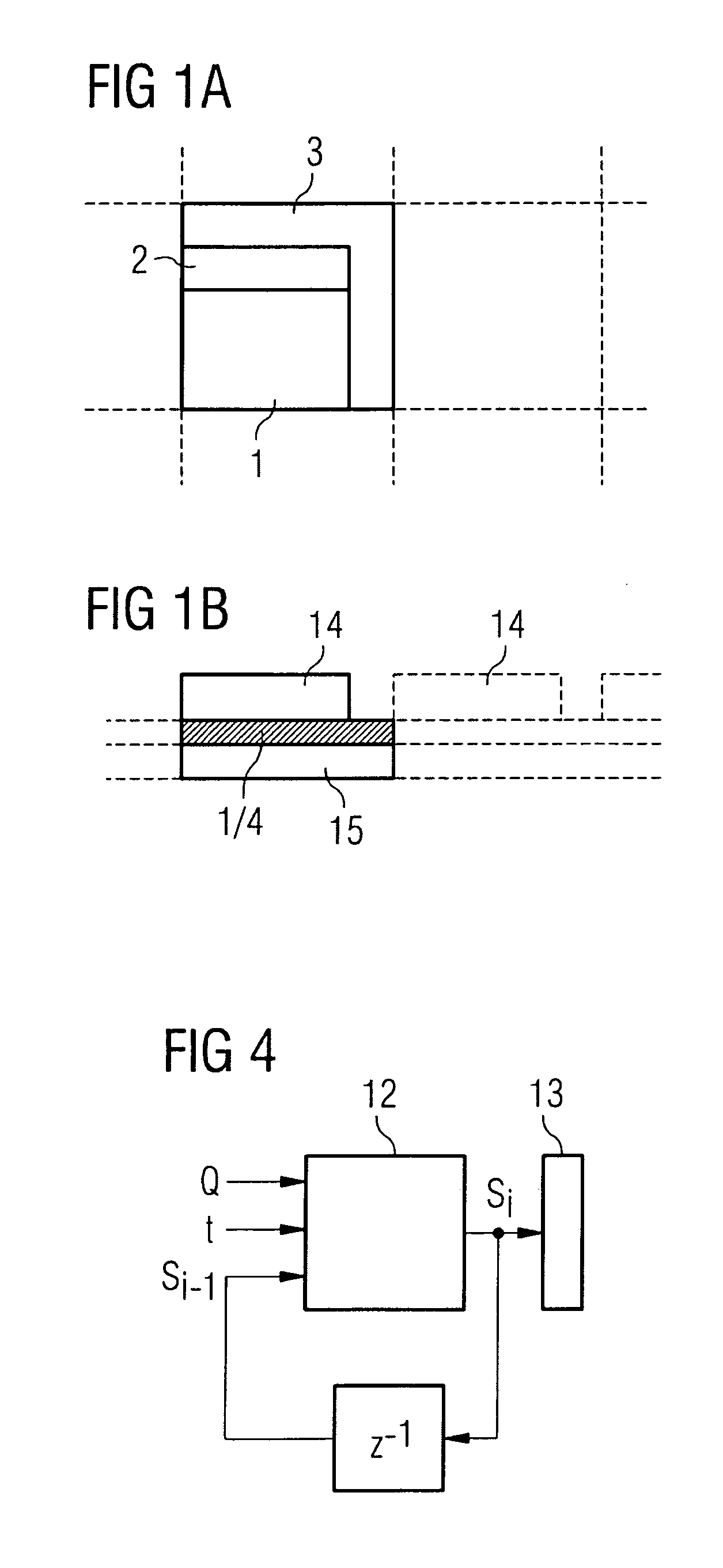
[0029]FIG. 1 shows an example of a basic cell of an (Active Pixel Sensor) APS measurement pixel in the form of a side view (FIG. 1b) and a plan view (FIG. 1a), as is used as the detector element in the present radiation detector. The radiation detector in this case includes a pixel matrix with m×n pixels (a section of which is indicated by dashed lines in the figure), which are produced on a CMOS silicon wafer as the mount substrate 15, with m and n preferably being greater than 10. The basic cell, which is illustrated by solid lines in FIG. 1, can be subdivided into three areas.
[0030] The first area includes the photosensitive area of the photosensor 1, which converts the incident light radiation to current. A structured scintillator 14 is arranged above the matrix of these basic cells, for conversion of X-ray radiation to visible light. Suitable scintillator materials are known to those skilled in the art, for example from the documents cited in the introduction to the descriptio...
PUM
 Abstract
Description
Claims
Application Information


