Semiconductor device and method of manufacturing the same
- Summary
- Abstract
- Description
- Claims
- Application Information
AI Technical Summary
Problems solved by technology
Method used
Image

Examples
first embodiment
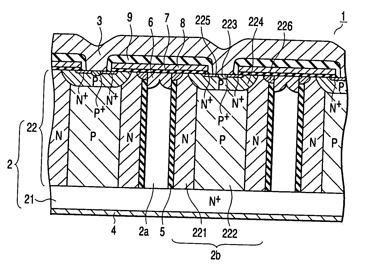
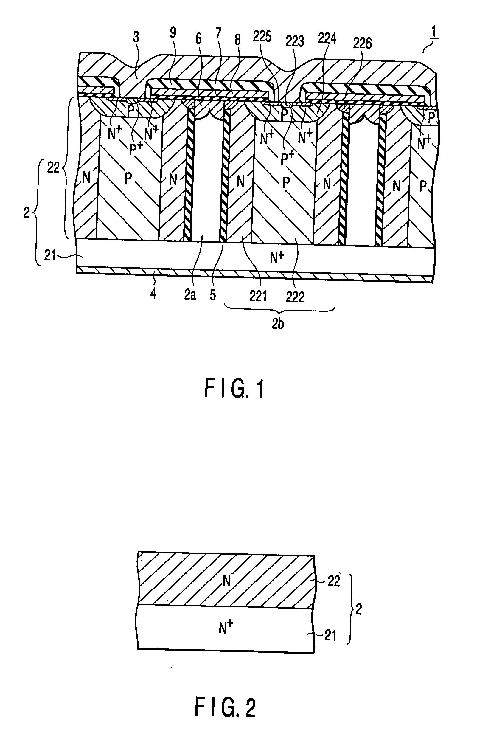
[0030]FIG. 1 is a sectional view schematically showing a semiconductor device according to the present invention. The semiconductor device 1 includes a vertical power MOSFET.
[0031] The semiconductor device 1 includes a semiconductor substrate 2. Trenches 2a are formed in one major surface of the semiconductor substrate 2. The trenches 2a form isolation regions, and define device regions 2b between the trenches 2a. The trenches 2a are typically very deep and have an aspect ratio of e.g., 20 or more.
[0032] A source electrode 3 is formed as a common electrode on the upper surface of the semiconductor substrate 2. A drain electrode 4 is formed as a common electrode on the lower surface of the semiconductor substrate 2. The semiconductor device 1 in FIG. 1 supplies a drain current in the direction of thickness of the semiconductor substrate 2, i.e., in the vertical direction.
[0033] The semiconductor substrate 2 includes a first semiconductor layer 21 of the first conductivity, N+-type ...
second embodiment
[0074] the present invention will be described.
[0075] In the first embodiment, epitaxial growth of Si occurs only near the opening of the trench 2a. In the second embodiment, epitaxial growth of Si also occurs on the upper surface of a substrate 2. A semiconductor device according to the second embodiment has almost the same structure as that of the semiconductor device according to the first embodiment except that a P+-type base region 224 and N+-type source region 225 are formed in a cap layer 6.
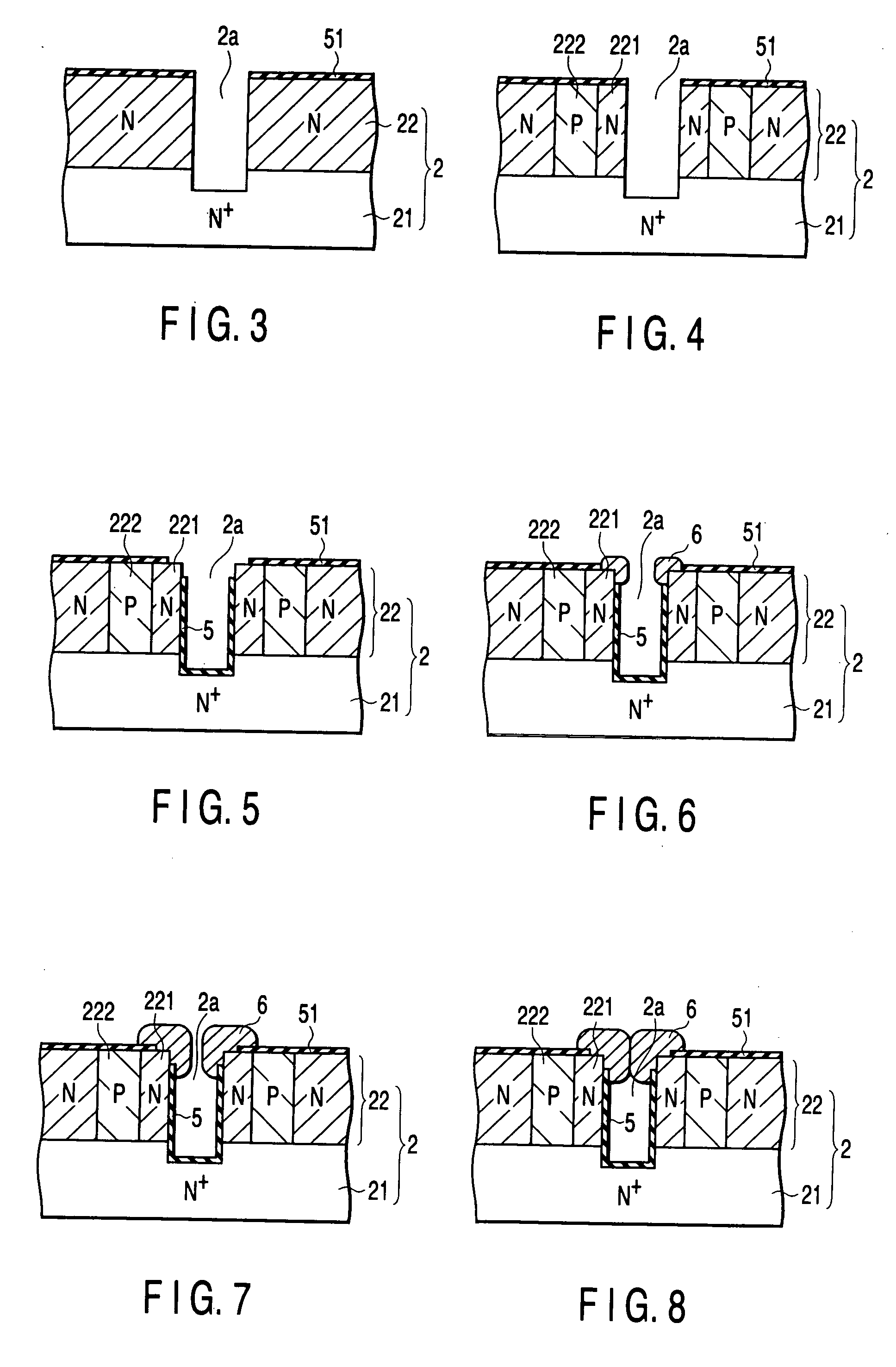
[0076] FIGS. 25 to 30 are sectional views schematically showing a method of manufacturing a semiconductor device according to the second embodiment of the present invention. FIGS. 25 to 30 assume that only one trench 2a is formed for illustrative convenience.
[0077] In this method, a structure shown in FIG. 4 is obtained by the same method as that described in the first embodiment.
[0078] As shown in FIG. 25, the exposed surface of a substrate 2 is oxidized to form a silicon oxide layer 5...
third embodiment
[0084] the present invention will be described.
[0085] In the first embodiment, portions of the oxide layer 5 and / or oxide layer 51 which are positioned at the boundary between the silicon oxide layer 51 and the sidewall of the trench 2a are removed, and Si is epitaxially grown on the exposed portions. In the third embodiment, a portion of an oxide layer 5 which is positioned on the sidewall of a trench 2a is partially removed, and Si is epitaxially grown at the exposed portion. A semiconductor device according to the third embodiment has almost the same structure as that of the semiconductor device according to the first embodiment except that an opening is formed in an insulating layer formed on the sidewall of the trench 2a.
[0086] FIGS. 31 to 37 are sectional views schematically showing a method of manufacturing a semiconductor device according to the third embodiment of the present invention. FIGS. 31 to 37 assume that only one trench 2a is formed for illustrative convenience.
[...
PUM
 Abstract
Description
Claims
Application Information
 - R&D
- Intellectual Property
- Life Sciences
- Materials
- Tech Scout
- Unparalleled Data Quality
- Higher Quality Content
- 60% Fewer Hallucinations
Browse by: Latest US Patents, China's latest patents, Technical Efficacy Thesaurus, Application Domain, Technology Topic, Popular Technical Reports.
© 2025 PatSnap. All rights reserved.Legal|Privacy policy|Modern Slavery Act Transparency Statement|Sitemap|About US| Contact US: help@patsnap.com