Optical tunable filter and method of manufacturing the same

a technology of optical tunable filters and manufacturing methods, applied in the direction of optical elements, waveguide devices, instruments, etc., can solve the problems of movable parts, drive electrodes can stick, and the driving becomes unstable, so as to simplify the manufacturing process of the first substrate

Inactive Publication Date: 2005-06-09
SEIKO EPSON CORP
View PDF4 Cites 25 Cited by
  • Summary
  • Abstract
  • Description
  • Claims
  • Application Information

AI Technical Summary

Benefits of technology

[0018] In this way, the movable part can be stably driven with a low voltage and structure of the optical tunable filter can be simplified as well as downsized. Furthermore, it is not necessary to provide a release hole and the optical tunable filter can be easily manufactured.
[0060] In this way, the first substrate with a mirrored surface can be easily obtained and a manufacturing process of the first substrate can be simplified.

Problems solved by technology

This can lead to a problem wherein driving becomes unstable because the thickness variation makes a coulomb force (electrostatic force) between a thin film and a drive electrode variable.
Furthermore, the thickness of the optical tunable filter is large since a movable part protrudes from a substrate (for example, see Japanese Unexamined Patent Publication No. 2002-174721).
However, there is a problem wherein the movable part and the drive electrode can stick to each other when a large electrostatic force is generated.
This decreases an area to which the coulomb force acts which causes a problem in that it increases a drive voltage.
Also, the stress induced warping of the high reflection film might occur at the movable part.
In addition, there is a problem in that the strength of the optical tunable filter might be reduced.

Method used


Image

  • Optical tunable filter and method of manufacturing the same
  • Optical tunable filter and method of manufacturing the same
  • Optical tunable filter and method of manufacturing the same

Examples


first embodiment

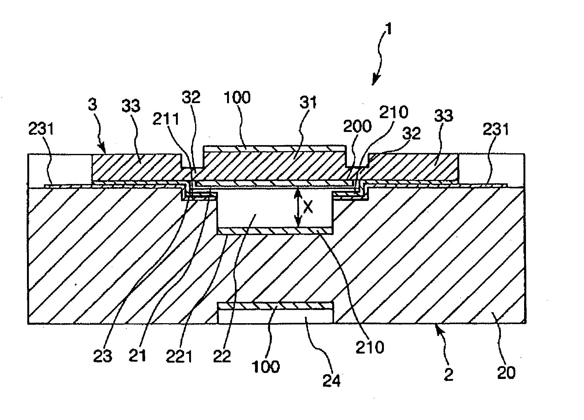
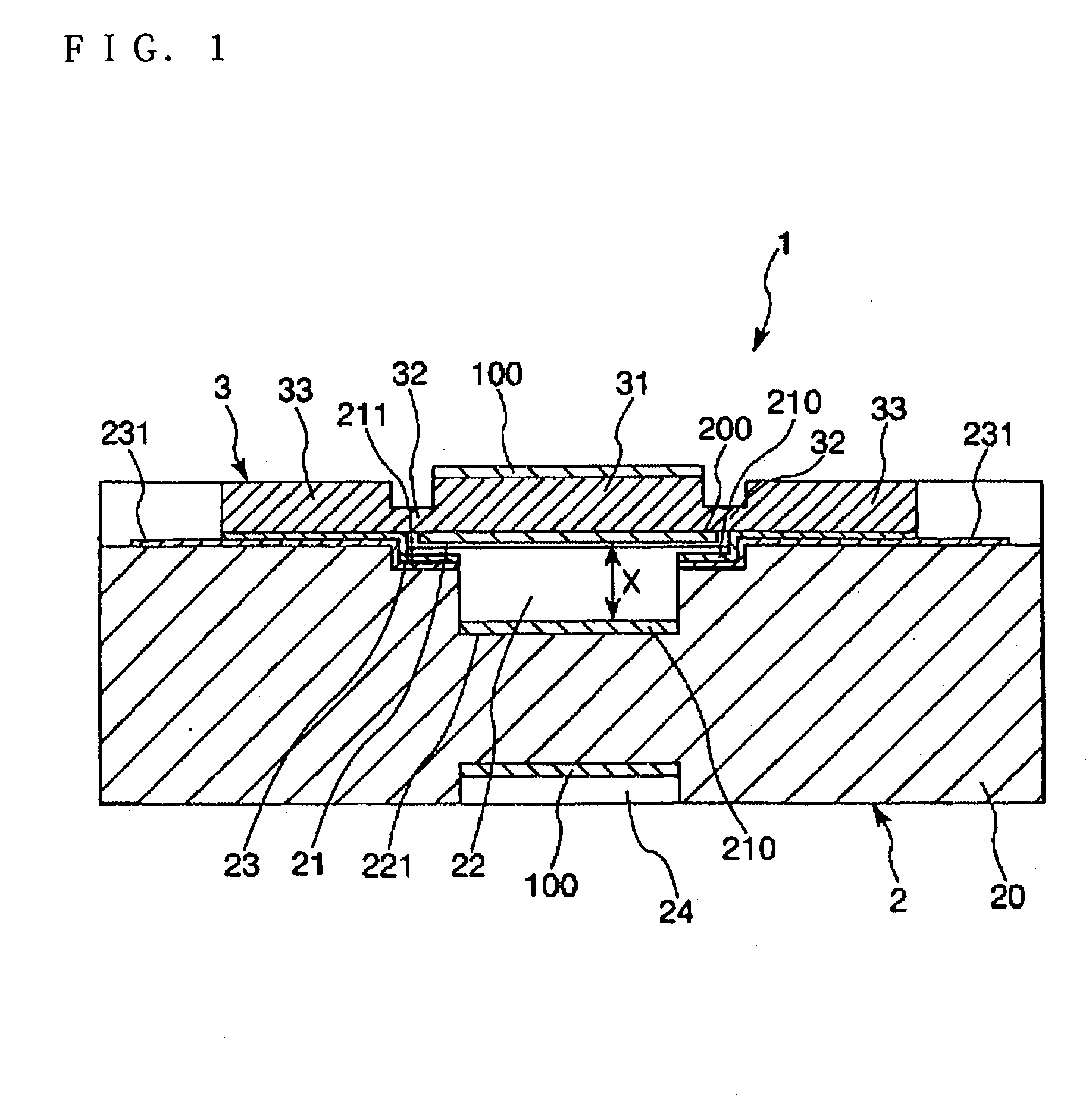
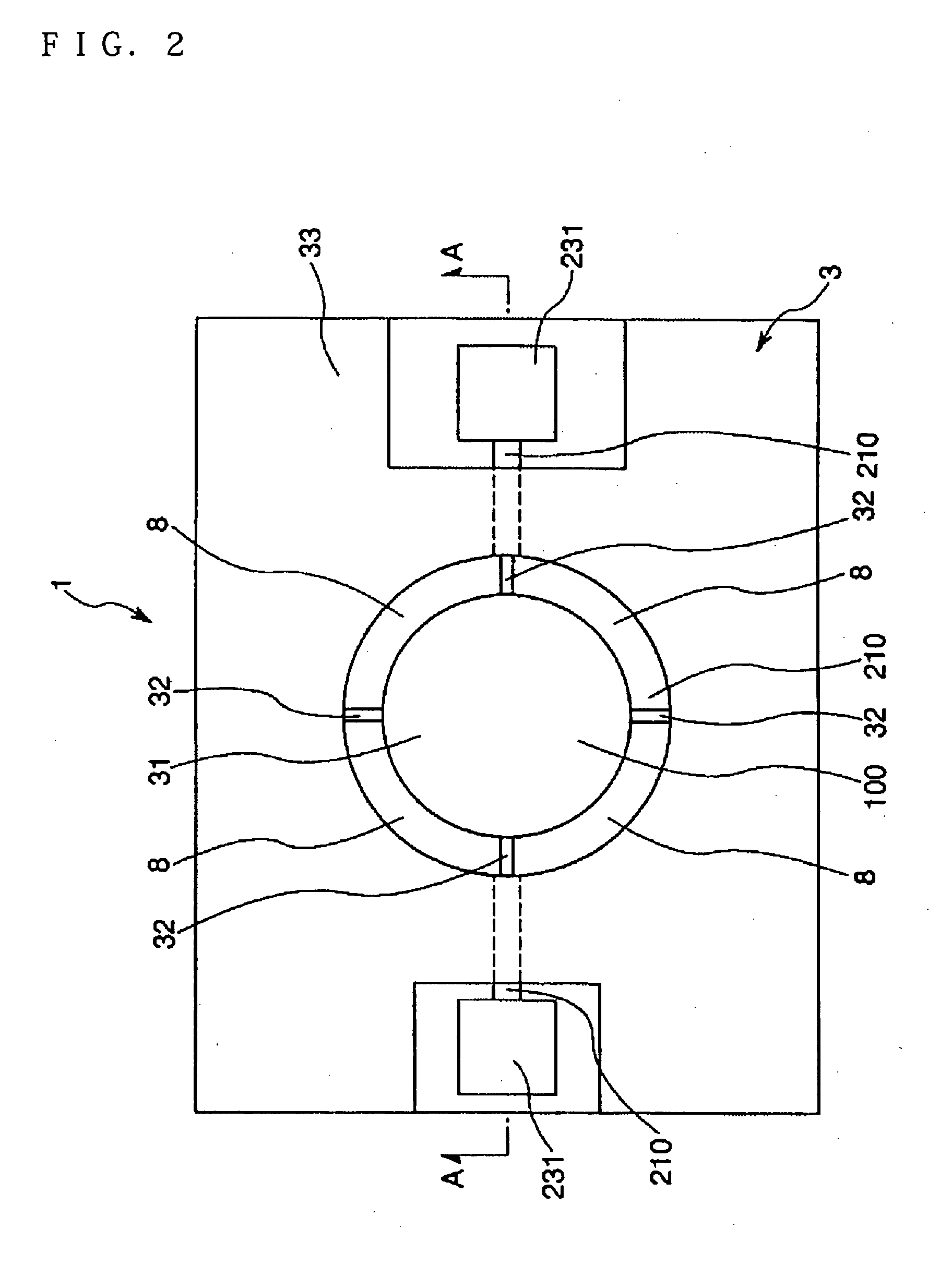
[0074]FIG. 1 is a sectional view of an optical tunable filter of a first embodiment along the line A-A of FIG. 2. FIG. 2 is a plan view of the optical tunable filter shown in FIG. 1. In the following description, the upper side of FIG. 1 is called “upward” and the lower side of FIG. 1 is called “downward”.

[0075] As shown in FIG. 1, an optical tunable filter 1 includes a first substrate 3 that is made of silicon, a base substrate 2 that is opposed to the first substrate 3, a first gap 21 and a second gap 22 that are provided between the first substrate 3 and the base substrate 2.

[0076] The first substrate 3 has conducting and light transmission properties. The first substrate 3 has a movable part 31 that is positioned in the middle, a supporting member 32 that supports the movable part 31 in a displaceable (movable) state and a conducting part 33 that turns on electricity to the movable part 31.

[0077] The movable part 31, the supporting member 32 and the conducting part 33 are form...

second embodiment

[0193] As shown in FIG. 7, in the optical tunable filter 1 of the second embodiment, an upper side (opposite side to the base substrate 2 side) of the movable part 31 and the conducting part 33 are coupled to the supporting member 32.

[0194] A manufacturing method is described below.

[0195] Manufacturing Method

[0196]FIGS. 8a and 8b are figures for explaining the manufacturing method of the second embodiment (schematically showing manufacturing processes). A feature of the manufacturing method according to the second embodiment is that the supporting member is made thin by processing from a lower side of the supporting member (a counter face side relative to the second base substrate 2 of the second Si layer 73). The manufacturing processes are the same as those of the first embodiment except process ′ is added after process in step (2) and process in step (4) is different. Process ′ in step (2) and process in step (4) are now described.

[0197]′ A photoresist pattern (not shown in...

third embodiment

[0202] As shown in FIG. 9, in the optical tunable filter 1 of the third embodiment, a center location of the movable part 31 and the conducting part 33 are coupled to the supporting member 32. A manufacturing method is described below.

[0203] Manufacturing Method

[0204]FIGS. 10a and 10b are figures for explaining the manufacturing method of the third embodiment (schematically showing manufacturing processes). A feature of the manufacturing method according to the third embodiment is that the supporting member is made thin by processing from the upper side and the lower side of the supporting member. The manufacturing processes are the same as those of the first embodiment except process ″ is added after process in step (2) and process in step (4) is different.

[0205] Process ″ in step (2) and process in step (4) are now described.

[0206]″ A photoresist pattern (not shown in the figures) is formed on the undersurface of the second Si layer 73 by photolithography and two-tiered anis...


PUM

PropertyMeasurementUnit
anglesaaaaaaaaaa
total thicknessaaaaaaaaaa
thicknessaaaaaaaaaa

Abstract

An optical tunable filter is provided including a first substrate having light transmission properties and having a movable part and a supporting member that movably supports the movable part and having a smaller thickness than the movable part, a second substrate having light transmission properties and opposed to the first substrate, a first gap and a second gap provided between the movable part and the second substrate, an interference part causing interference between the movable part and the second substrate through the second gap and a drive member changing an interval of the second gap by moving the movable part to the second substrate by making use of the first gap.

Description

RELATED APPLICATIONS [0001] This application claims priority to Japanese Patent Application No. 2003-405247 filed Dec. 3, 2003 which is hereby expressly incorporated by reference herein in its entirety. BACKGROUND [0002] 1. Field of the Invention [0003] The present invention relates to an optical tunable filter and a method of manufacturing the same. [0004] 2. Related Art [0005] The following applications relate to the optical tunable filter according to the present invention. [0006] Filter by Surface Micro-Machining Technology [0007] In a conventional optical tunable filter, the thickness of a sacrificial layer solely controls the thickness of a variable gap therein. According to this technology, however, the thickness of the sacrificial layer widely varies depending on forming conditions. This can lead to a problem wherein driving becomes unstable because the thickness variation makes a coulomb force (electrostatic force) between a thin film and a drive electrode variable. Further...

Claims


Application Information

Patent Timeline
Patent Type & Authority Applications(United States)
IPC IPC(8): B81B3/00G02B5/20B81C1/00G01J3/26G02B5/28G02B26/00H01P1/20
CPCG02B26/001G01J3/26G02B1/11G02B5/28
Inventor NAKAMURA, RYOSUKEKAMISUKI, SHINICHIMURATA, AKIHIROYODA, MITSUHIRO
Owner SEIKO EPSON CORP
Why Eureka
Try Eureka