Surface emitting and receiving photonic device with lens

a photonic device and surface technology, applied in semiconductor laser arrangements, optical resonator shape and construction, semiconductor lasers, etc., can solve the problems of incompatible monolithic integration, inability to test devices in full-wafer, and same deficiencies, so as to facilitate laser operation monitoring

Active Publication Date: 2005-06-09
MACOM TECH SOLUTIONS HLDG INC
View PDF7 Cites 62 Cited by
  • Summary
  • Abstract
  • Description
  • Claims
  • Application Information

AI Technical Summary

Benefits of technology

[0008] In accordance with the present invention, improved surface emitting semiconductor lasers are provided in which light is emitted at an emitter end of an optical cavity in a direction vertical to the plane of the laser active layer, and in which light is emitted at a reflective region at the opposite end of the cavity in the plane of the active layer. This arrangement facilitates monitoring of laser operation without adversely affecting the light output. In accordance with one form of the invention, a reflection modification layer or stack is provided on the emitter end while in another form of the invention filter elements are provided within the laser cavity, to permit operation of the laser in an essentially single longitudinal mode. Furthermore, in accordance with the invention, surface and in-plane detectors are provided on the same substrate as the laser, and multiple laser cavities are positioned to enable the emission of multiple wavelengths at a common location.
[0010] The upper contact layer, which may be a low bandgap semiconductor material to allow ohmic contacts to be formed, preferably incorporates an aperture in the region of the angled facet to remove light-absorbing layers from the surface and to improve the efficiency of the device.
[0013] In accordance with another embodiment of the invention, an optical detector is located on the substrate beside the laser and is integrally formed with the laser in that it uses the same epitaxial structure on the substrate as is used for the laser. In this case, the epitaxial layers are etched during the etching of the laser cavity to fabricate a detector region that occupies a surface of the substrate adjacent to the laser. Suitable electrodes are deposited on the detector region so that light that impinges on it will be detected. This allows both a light emitter and a light detector to be integrally formed on a single substrate side-by-side.
[0014] In still another embodiment of the invention the light detector is an integral in-plane detector with a 45° angled facet which is located beside the laser and is fabricated from the same epitaxial structure as is used for the laser. The detector is elongated, and may be generally parallel to the laser axis to conserve space on the substrate. The light to be detected impinges on the detector surface above the angled facet, and is directed into the active region of the detector through the total internal reflection of the angled facet. This surface-receiving detector can be made to be extremely fast by controlling its length and width. The surface above the 45°-angled facet that is parallel to the active layers may be coated with a dielectric layer or stack to make it antireflective for even better operation of the detector.
[0015] In order to provide a selectable wavelength output, in accordance with another embodiment of the invention, multiple surface emission laser cavities may be positioned so that their emitting ends are clustered adjacent to each other, with the cavities extending outwardly; for example, as spokes surrounding a central hub. The epitaxial structure in each laser device may be slightly different to cause a different wavelength to be emitted from each one. The proximity of the emitting ends then allows the outputs from all of the lasers to be easily combined into one receiving medium, such as a fiber, and by selectively activating the lasers, a selected wavelength, or wavelengths, can be transferred into the fiber.
[0018] A problem common to the various embodiments described above is that of divergence of the propagating light in the laser, produced at the angled facet. The light generated in the laser cavity travels axially along the cavity and is reflected upwardly by the angled facet to produce an emitted beam that is perpendicular to the cavity axis. The reflected light experiences diffraction at the totally internally reflective facet and diverges as it travels upwardly through the upper cladding layer of the laser. The light strikes the upper partially reflective top surface of the laser, some light is emitted, and the remaining light is reflected back toward the angled facet. The returned light further diverges, so that only a portion of that light is coupled back into the optical cavity, or waveguide, of the laser in a guided mode. This reduces the efficiency of the laser.

Problems solved by technology

The resultant devices cannot be tested in full-wafer and as such suffer from the same deficiencies as cleaved facet devices.
Furthermore, they are incompatible with monolithic integration in view of the need for cleaving.
Chao, et al., IEEE Photonics Technology Letters, volume 7, pages 836-838, attempted to overcome these short-comings, however, by providing an interrupted waveguide structure, but the resultant device suffered from scatter at each end of the laser cavity.
Vertical Cavity Surface Emitting Lasers (VCSELs) have gained popularity over the past several years; however, VCSELs do not allow in-plane monolithic integration of multiple devices and only allow light to exit their surface mirror at perpendicular incidence.

Method used


Image

  • Surface emitting and receiving photonic device with lens
  • Surface emitting and receiving photonic device with lens
  • Surface emitting and receiving photonic device with lens

Examples


Embodiment Construction

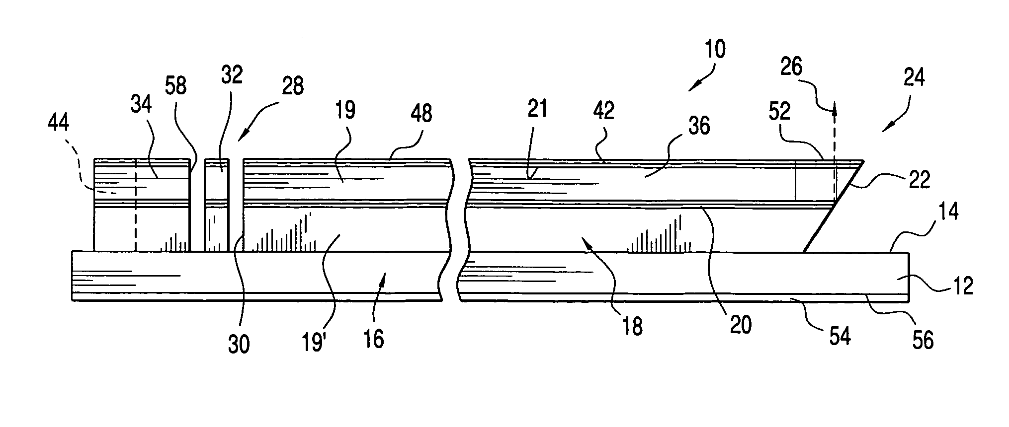
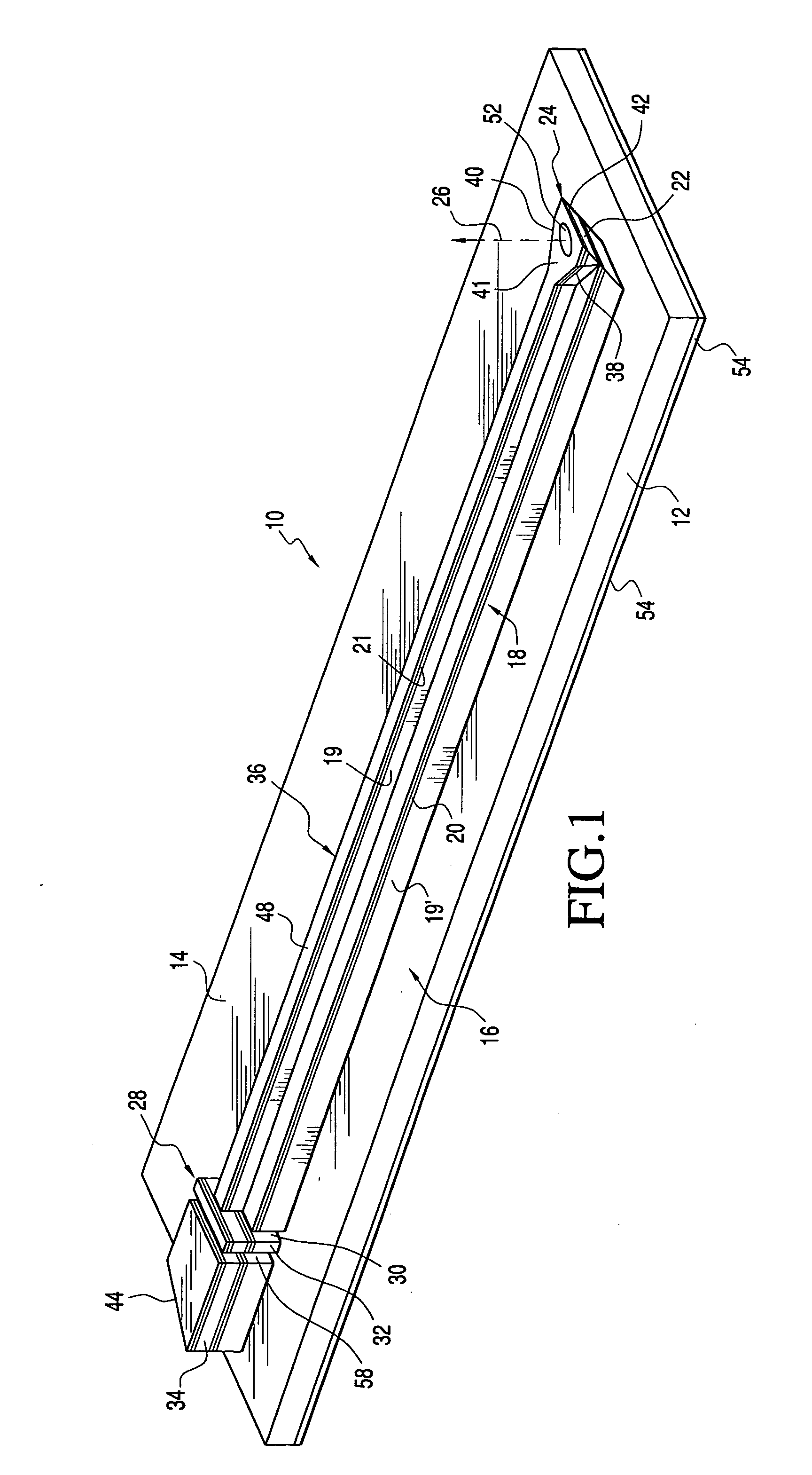
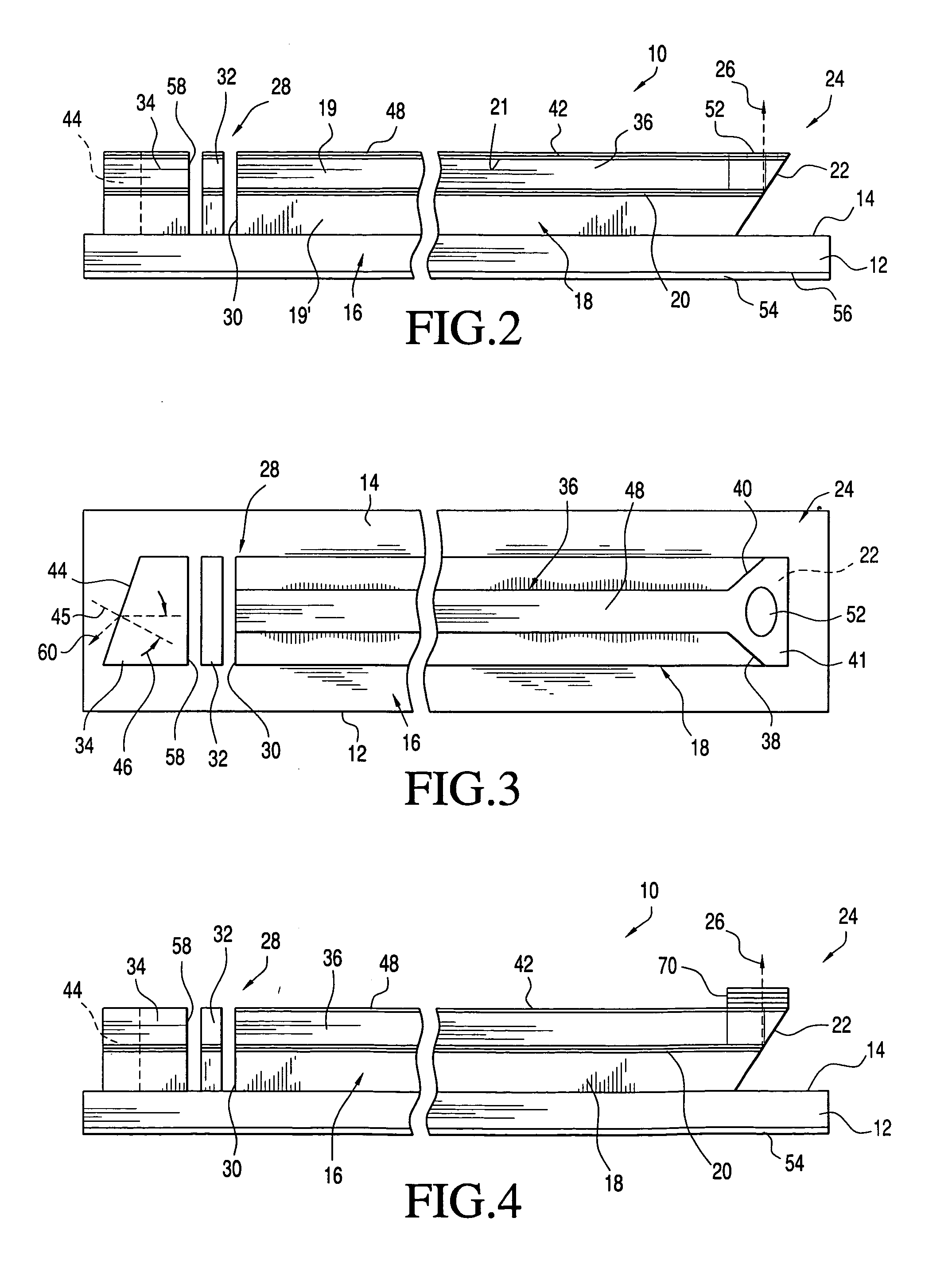
[0043] Turning now to a more detailed description of the invention, a surface emitting semiconductor laser 10 fabricated on a substrate 12 is illustrated diagrammatically in FIGS. 1-3. Although the invention will be described in terms of a ridge laser, it will be understood that other types of lasers may be fabricated utilizing the features of the invention as herein described.

[0044] As is conventional in the fabrication of solid state ridge lasers, the substrate 12 may be formed, for example, of a type III-V compound, or an alloy thereof, which may be suitably doped. The substrate includes a top surface 14 on which is deposited, as by an epitaxial deposition such as Metalorganic Chemical Vapor Deposition (MOCVD) or Molecular Beam Epitaxy (MBE), a succession of layers generally indicated at 16 which form an optical cavity 18 that includes an active region 20. A horizontal cavity semiconductor laser structure such as the optical cavity 18 typically contains upper and lower cladding ...


PUM


Abstract

A surface-emitting laser, in which light is emitted vertically at one end from a near 45°-angled facet, includes a second end having a perpendicular facet from which light is emitted horizontally, for monitoring. The surface-emitting laser comprises a divergence-compensating lens on the surface above the near 45°-angled facet.

Description

BACKGROUND OF THE INVENTION [0001] This application claims the benefit of U.S. Provisional Application No. 60 / 512,189, filed Oct. 20, 2003, and of U.S. Provisional Application No. 60 / 578,289, filed Jun. 10, 2004, the disclosures of which are hereby incorporated herein by reference. [0002] The present invention relates, in general to improved surface emitting and receiving photonic devices and methods for fabricating them, and more particularly to surface emitting photonic devices incorporating a lens for improved efficiency. [0003] Semiconductor lasers typically are fabricated by growing the appropriate layered semiconductor material on a substrate through Metalorganic Chemical Vapor Deposition (MOCVD) or Molecular Beam Epitaxy (MBE) to form an active layer parallel to the substrate surface. The material is then processed with a variety of semiconductor processing tools to produce a laser optical cavity incorporating the active layer, and metallic contacts are attached to the semico...

Claims


Application Information

Patent Timeline
Patent Type & Authority Applications(United States)
IPC IPC(8): H01SH01S3/08H01S5/00H01S5/026H01S5/0683H01S5/125H01S5/14H01S5/185H01S5/22H01S5/223H01S5/40H01S5/42
CPCH01S5/02284H01S5/42H01S5/0262H01S5/0264H01S5/0267H01S5/0654H01S5/0683H01S5/1014H01S5/1085H01S5/125H01S5/141H01S5/18H01S5/22H01S5/2231H01S5/4012H01S5/026H01S5/02251H01S5/185
Inventor BEHFAR, ALEX A.SCHREMER, ALFRED T.STAGARESCU, CRISTIAN B.
Owner MACOM TECH SOLUTIONS HLDG INC
Why Eureka
Try Eureka