Method and apparatus for depositing charge and/or nanoparticles

a charge and/or nanoparticle technology, applied in the field of nanoparticles, can solve the problems of serial techniques, lag in yield and speed, and devices that do not hold the only interest in nanoparticle generation,

Active Publication Date: 2005-06-09
RGT UNIV OF MINNESOTA
View PDF16 Cites 42 Cited by
  • Summary
  • Abstract
  • Description
  • Claims
  • Application Information

AI Technical Summary

Problems solved by technology

However, devices do not hold the only interest in nanoparticle generation.
However, inherent disadvantages such as the lag in yield and speed, will have to be overcome in the future to enable the manufacturing of nanotechnological devices.
Serial techniques, however, remain slow—the fastest scanning probe-based system needs 1.5 days to pattern an area of 1 cm2.

Method used


Image

  • Method and apparatus for depositing charge and/or nanoparticles
  • Method and apparatus for depositing charge and/or nanoparticles
  • Method and apparatus for depositing charge and/or nanoparticles

Examples


Embodiment Construction

[0025] Non-Traditional Parallel Nanofabrication is a fast growing field that uses alternative methods to fabricate and pattern nanostructures at low cost. It is believed that these techniques will become an important part of future micro- and nanofabrication. Most of these techniques use a master to replicate nanostructures in parallel. Current research focuses on microcontact printing, molding, embossing, near-field photolithography topographically directed etching and topographically directed photolithography.

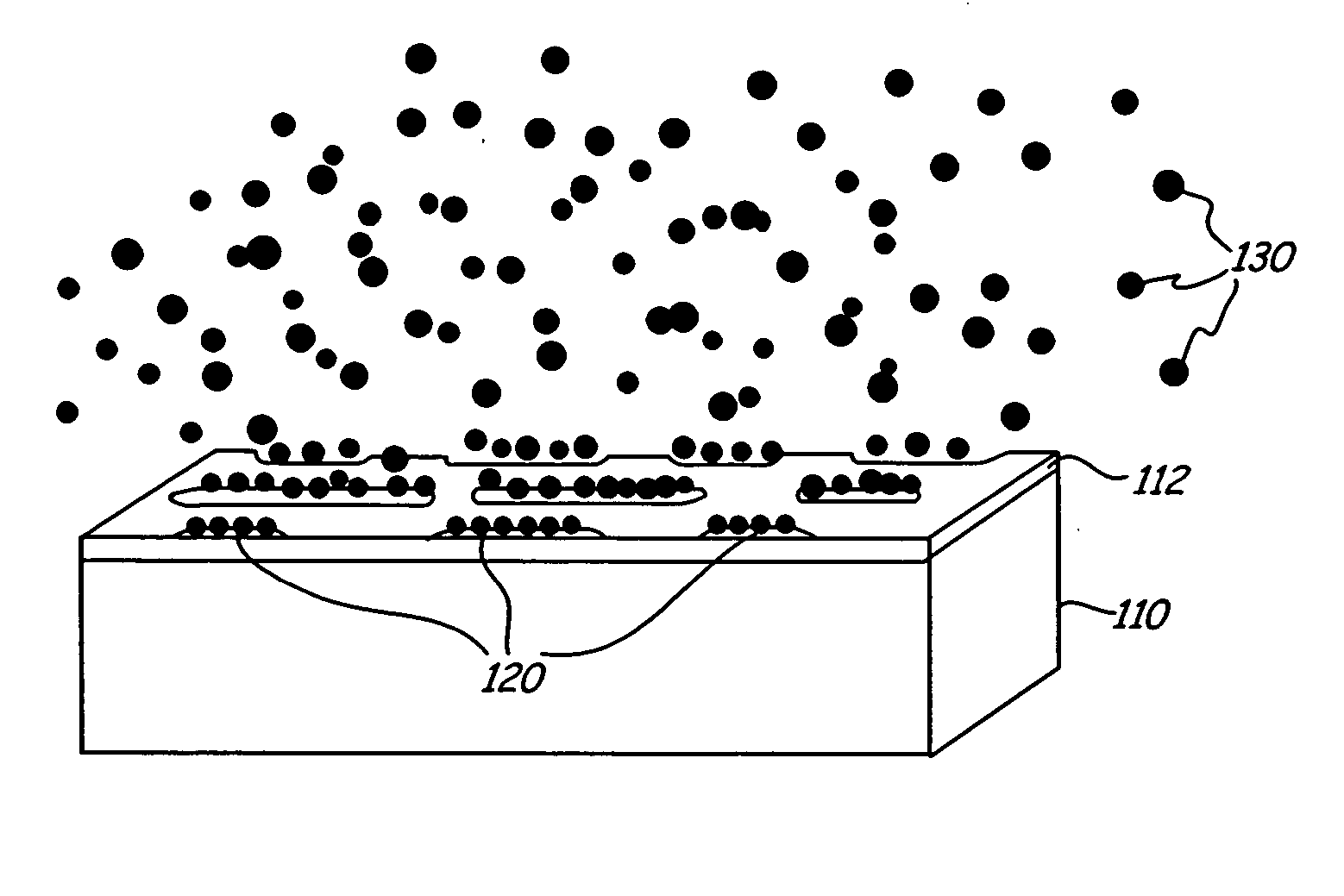
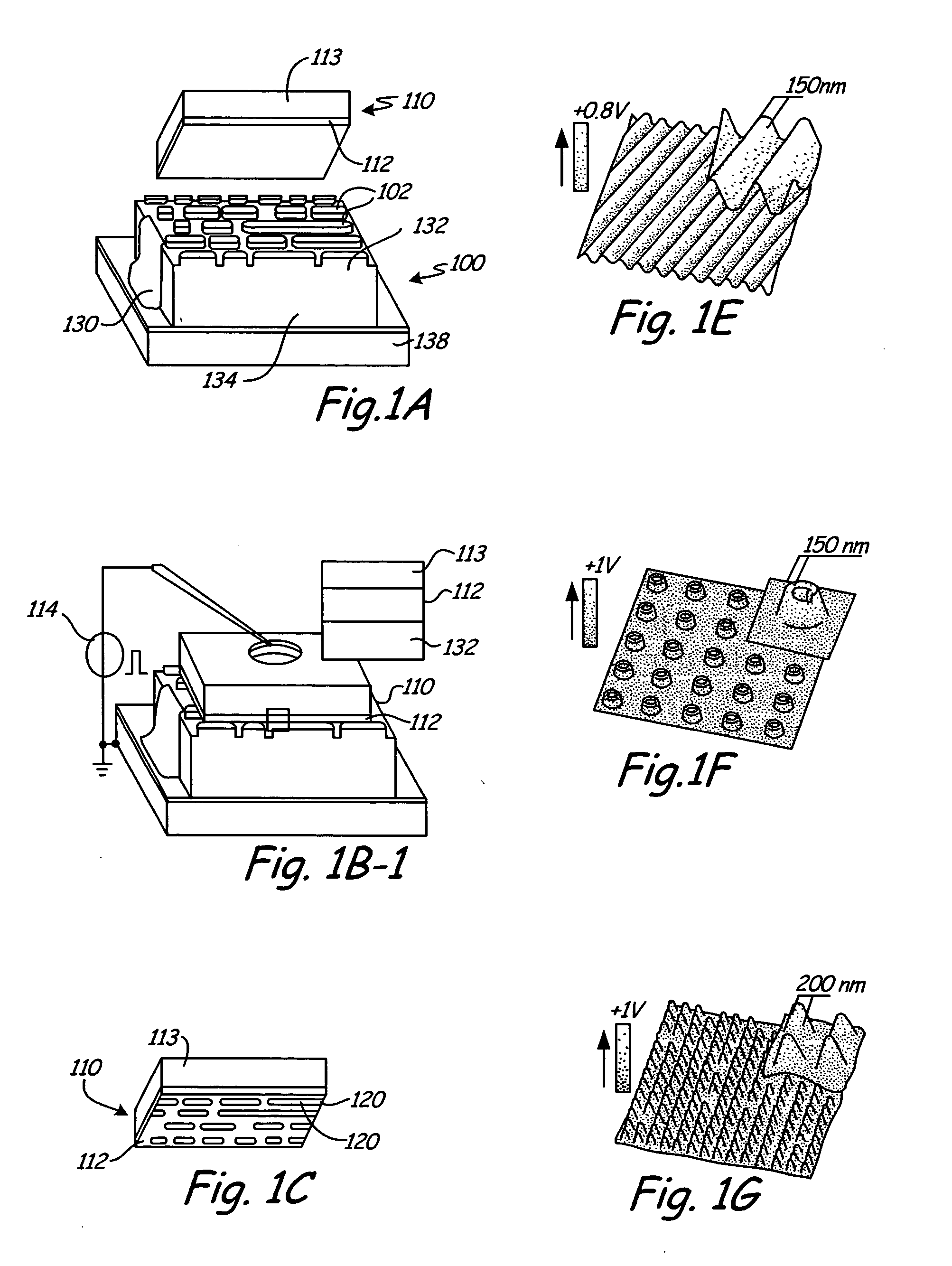
[0026]FIGS. 1A, 1B and 1C illustrate steps of a stamping process in accordance with one aspect of the present invention. A flexible conducting stamp 100 is illustrated which includes surface features 102 formed thereon. FIG. 1B is a perspective view showing stamp 100 positioned in contact with a rigid support substrate 110. Rigid support substrate 110 is covered by a layer of photoresist, electret or other material 112 carried on conductive support 113 and a voltage pulse is...


PUM


Abstract

A method and apparatus for use in depositing electrical charge and / or nanoparticles is provided. A stamping process is used in which a stamp having a flexible layer such as a flexible semiconductor layer applies a charge pattern on a substrate. Other techniques include lithographic patterning, the use of pre-patterned dissimilar materials, deposition by ions or radiation, the use of differing work functions, the use of liquid phase materials. Deposition monitoring techniques and apparatuses are also provided.

Description

[0001] The present application is based on and claims the benefit of U.S. provisional patent application Ser. No. 60 / 517,327, filed Nov. 4, 2003, the content of which is hereby incorporated by reference in its entirety.GOVERNMENT RIGHTS [0002] The United States government has certain rights in this invention pursuant to Agency Grant No. DMI-0217538 awarded by DMII Grant NSF.BACKGROUND OF THE INVENTION [0003] The present invention relates to nanoparticles. More specifically, the present invention relates to the deposition of charge and / or nanoparticles. [0004] There is an ongoing trend to miniaturize components and devices. Smaller components and devices allow more complex functions to be performed in a smaller volume and, in some configurations, can increase speed and reduce power consumption of a device. Small components have also found use in the biological and medical sciences. Today's forefront of miniaturization is generally referred to as “nanotechnology”. One technique used i...

Claims


Application Information

Patent Timeline
Patent Type & Authority Applications(United States)
IPC IPC(8): B05D1/12B05D5/00G03G5/02G03G5/153
CPCG03G5/02Y10S977/901G03G5/153
Inventor JACOBS, HEIKO O.BARRY, CHAD
Owner RGT UNIV OF MINNESOTA
Why Eureka
Try Eureka