Photo mask capable of improving resolution by utilizing polarization of light and method of manufacturing the same

Inactive Publication Date: 2005-06-09
SAMSUNG ELECTRONICS CO LTD
View PDF5 Cites 9 Cited by
  • Summary
  • Abstract
  • Description
  • Claims
  • Application Information

AI Technical Summary

Benefits of technology

[0011] An object of the present invention is to provide a photo mask that can enhance the resol

Problems solved by technology

However, many problems exist in the mass-production of ArF light sources and the like.
Nonetheless, such a light-blocking pattern requires an additional process that increases the Turn Around Time (TAT) for manufacturing the mask.
Also, an Mo film causes a haze to develop on the mask.
However, it is impossible to completely prevent a haze from eventua

Method used


Image

  • Photo mask capable of improving resolution by utilizing polarization of light and method of manufacturing the same
  • Photo mask capable of improving resolution by utilizing polarization of light and method of manufacturing the same
  • Photo mask capable of improving resolution by utilizing polarization of light and method of manufacturing the same

Examples


experimental example 1

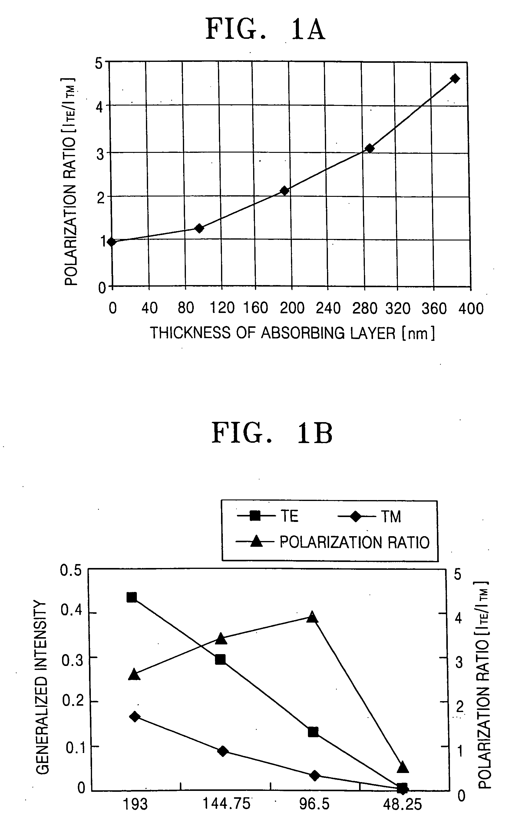
[0045] Hereinafter, changes in contrast according to changes in the thickness of the external reflection pattern will be described with reference to simulations, the results of which are shown in FIG. 6. Graph (a) of FIG. 6 shows generalized intensity changes of a TE wave, a TM wave and a TEM wave obtained through a simulation in which a conventional BM is used. Graph (b) of FIG. 6 shows generalized intensity changes of a TE wave, a TM wave and a TEM wave obtained through a simulation in which a photo mask including a reflection pattern having a thickness of 240 nm according to the present invention is used. The simulations were carried out using a lens with a numerical aperture (NA) of 0.8, an annular aperture of 0.59 / 0.89 and a line and space pattern of 140 nm. The reflection pattern is made of SOG, the transparent substrate is a quartz substrate, and the light-blocking pattern is a chrome pattern.

[0046] In the case of the BM, the TM wave has a lower maximum intensity and a highe...

experimental example 2

[0048]FIG. 8 is a graph showing changes in the reduction ratio of minimum intensity and corresponding changes in contrast, according to changes in the thickness of a SOG pattern, with respect to a pattern having a pitch of 140 nm. The conditions of this simulation are same as in Experimental Example 1 except that the pattern is a hole-shaped contact pattern.

[0049] Referring to FIG. 8, the reduction ratios of the minimum intensity, with respect to an X direction and a Y direction perpendicular to the X direction, decrease as the SOG pattern becomes thinner, and become nearly constant once the thickness exceeds about 120 nm. Accordingly, FIG. 8 shows that the contrast becomes maximum when the thickness of the SOG pattern is 120 nm. Also, FIG. 8 shows that enhanced contrast is achieved when the SOG pattern is thinner than 240 nm (the thickness of a phase shift film). This is because with respect to a contact pattern, the reflection pattern would be formed on four sides in the light-tr...


PUM


Abstract

A photo mask enhances the resolution of a photolithography process by polarizing the exposure light. The photo mask includes a transparent substrate made of quartz, a reflection pattern disposed on the transparent substrate, and a light-blocking pattern disposed on the reflection pattern. The external reflection pattern defines a light-transmitting area by exposing portions of the transparent substrate. The light-blocking pattern has the same size and shape as the external reflection pattern.

Description

BACKGROUND OF THE INVENTION [0001] 1. Field of the Invention [0002] The present invention relates to the process of photolithography used in the manufacturing of semiconductor devices and the like. More particularly, the present invention relates to a photo mask and to a method of manufacturing the same. [0003] 2. Description of the Related Art [0004] Process margins in the manufacturing of semiconductor devices are becoming smaller and smaller as the design rule of the devices has decreased to meet the demand for more highly integrated devices. One semiconductor manufacturing process that is being refined is photolithography. In photolithography, light of a given wavelength is directed from a light source onto a substrate through a photo mask such that an image of the photo mask is projected onto the substrate. The image is developed and exposed to form a pattern on the substrate. Conventionally, a KrF light source has been widely used as the light source, and a binary mask (BM) ha...

Claims


Application Information

Patent Timeline
IPC IPC(8): G03F1/14G03F9/00G21K5/00H01L21/027
CPCG03F1/14G03F1/38G03F1/50H01L21/027
Inventor KIM, SUNG-HYUCKSHIN, IN-KYUNYOON, GI-SUNG
Owner SAMSUNG ELECTRONICS CO LTD
Why Eureka
Try Eureka