3D polysilicon ROM and method of fabrication thereof

a polysilicon rom and polysilicon technology, applied in the field of polysilicon read only memory (rom), can solve the problems of difficult control of programming voltage, high antifuse breakdown voltage between two polysilicon layers, and difficult to define antifuse breakdown if the antifuse material is uniform and rough, etc., to reduce the required antifuse breakdown voltage and improve processing yield

Active Publication Date: 2005-06-09
MACRONIX INT CO LTD
View PDF1 Cites 82 Cited by
  • Summary
  • Abstract
  • Description
  • Claims
  • Application Information

AI Technical Summary

Benefits of technology

[0009] In view of the foregoing, it is an object of the present invention to provide a 3D polysilicon ROM to decrease the required antifuse breakdown voltage which is applied for the occurrence of current breakdown with high electrical breakdown field between two polysilicon layers. And the invention also could well confine the memory cell and well confine the breakdown region so that yield in processing can be improved.

Problems solved by technology

However, the antifuse breakdown voltage is high between two polysilicon layers in the conventional 3D polysilicon ROM.
In general, the oxide breakdown voltage is high, so it's a key issue to reduce programming voltage.
Moreover, the antifuse breakdown is hard to define if the antifuse material is uniform and rough.
The antifuse breakdown region is hard to define, so the programming voltages are difficult to be controlled.
Hence, the yield in array architectures is low.

Method used


Image

  • 3D polysilicon ROM and method of fabrication thereof
  • 3D polysilicon ROM and method of fabrication thereof
  • 3D polysilicon ROM and method of fabrication thereof

Examples


example 1

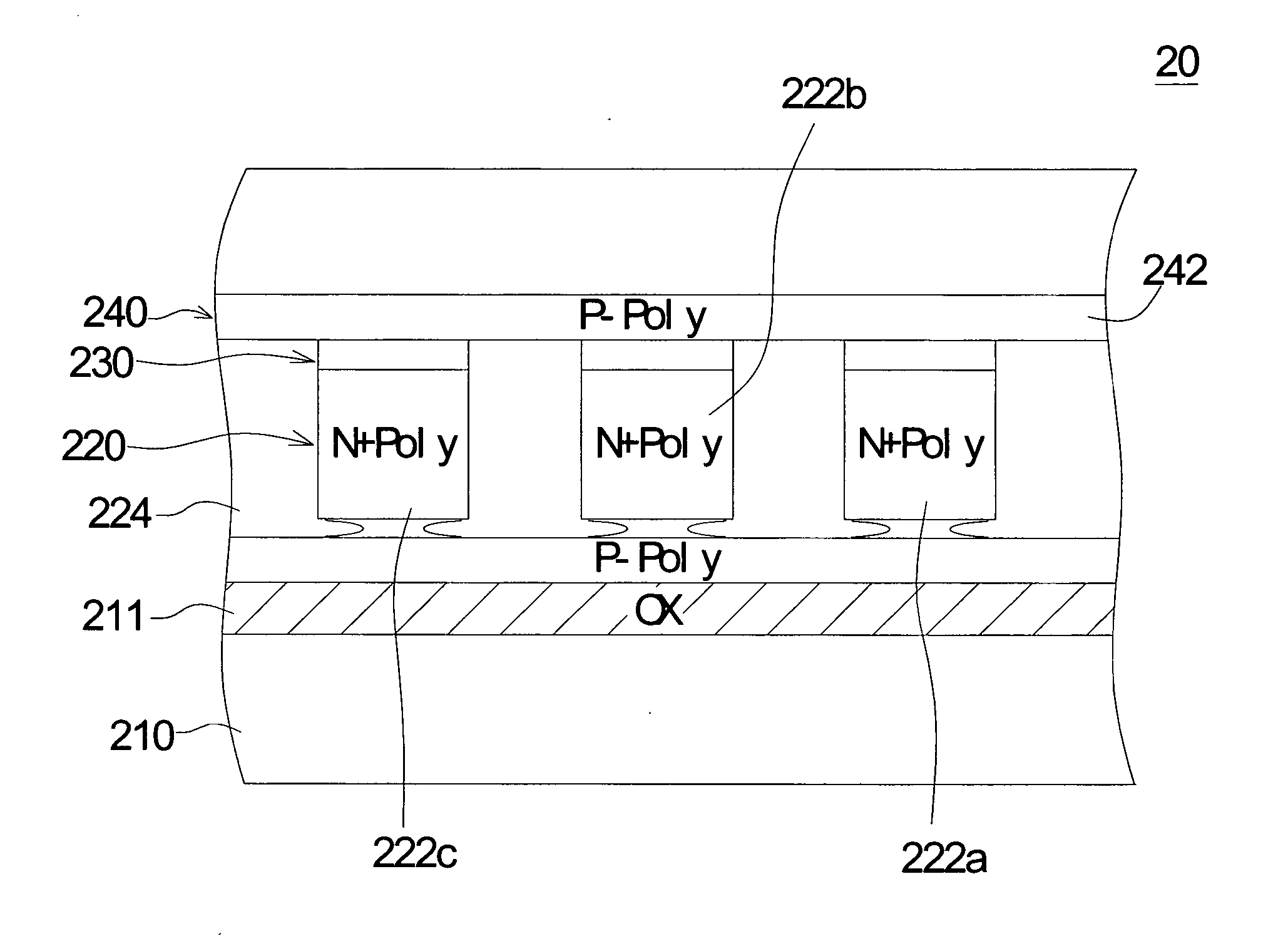
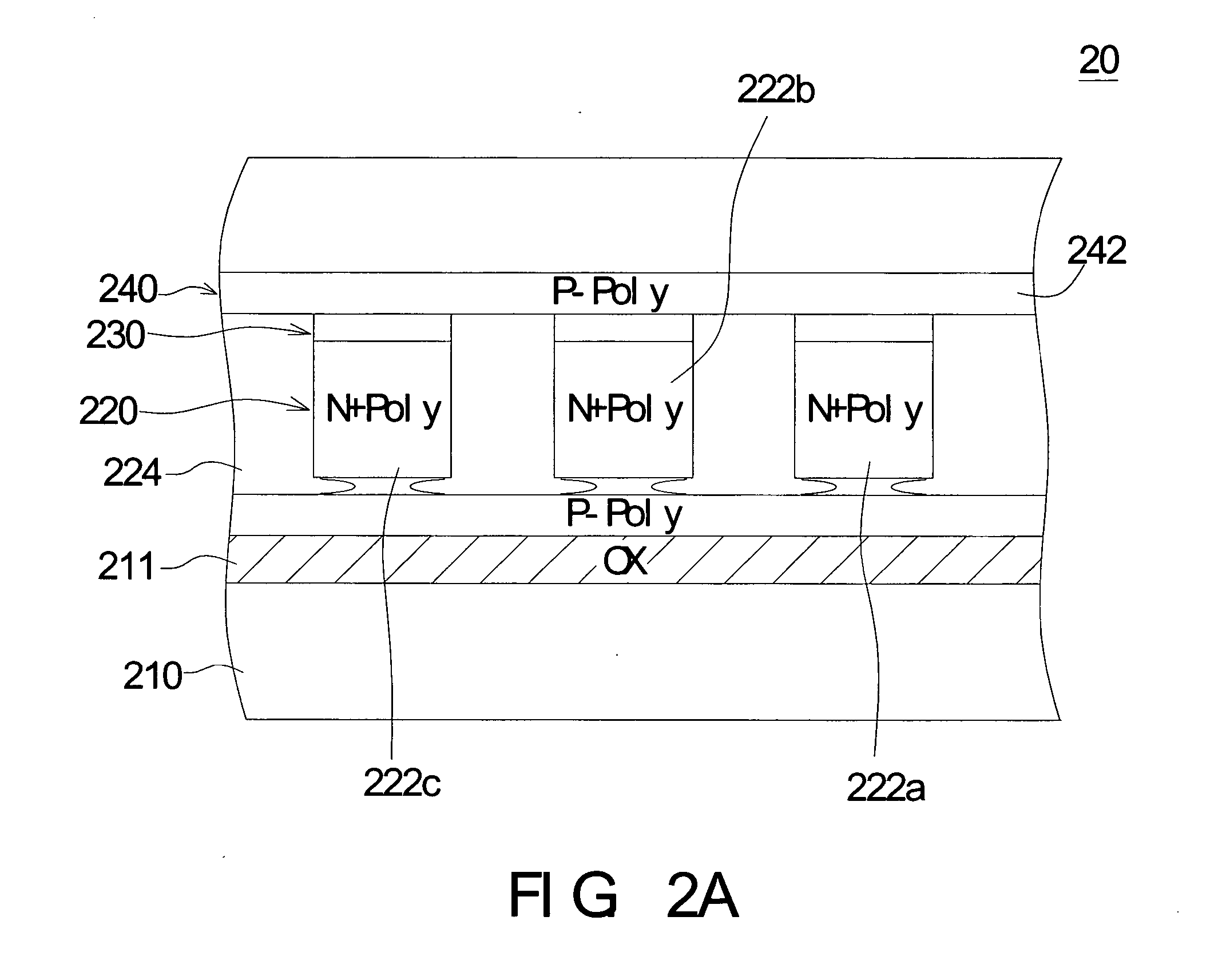
[0020]FIG. 2A is a cross-sectional view showing a 3D polysilicon ROM of the first example of the invention. Referring first to FIG. 2A, a 3D polysilicon read only memory (ROM) 20 includes a silicon substrate 210, an isolated silicon dioxide (SiO2) layer 211, a N-Type heavily doped (N+) polysilicon layer 220, a dielectric layer 230, a P-Type lightly doped (P−) polysilicon layers 240, a first oxide layer 224, and a second oxide layer 244.

[0021] The isolated SiO2 layer 211 is deposited on the silicon substrate 210, and the N-Type heavily doped (N+) polysilicon layer 220 is deposited on the isolated SiO2 layer 211. The N+ polysilicon layer 220 is further defined a plurality of parallel, separate word lines (WL), such as word lines 222a, 222b, 222c in FIG. 2A. The first oxide layer 224 is filled in the space between the word lines 222a, 222b, 222c. The dielectric layer 230 is deposited on the word lines 222a, 222b, 222c and on the first oxide layer 224.

[0022] The P-Type lightly doped (...

example 2

[0029]FIG. 3A is a flow chart showing the method of fabrication for the 3D polysilicon ROM according to the second embodiment of the invention, and FIG. 3B to 3F are cross-sectional views showing the process steps of the second embodiment of the method of fabrication for the 3D polysilicon ROM. Referring first to FIG. 3F, a 3D polysilicon read only memory (ROM) 30 includes a silicon substrate 310, an isolated silicon dioxide (SiO2) layer 311, a N-Type heavily doped (N+) polysilicon layer 320, a dielectric layer 330, P-Type lightly doped (P−) polysilicon layers 340, 350, and oxide layers 344,354.

[0030] The method of fabrication for the 3D polysilicon ROM according to the second embodiment of the invention is described below. First, as described in step 361, a silicon substrate 310 is provided. Then, as described in step 363, an isolated SiO2 layer 311 is deposited on the substrate 310. As described in step 365, a N-Type heavily doped (N+) polysilicon layer 320 is formed on the isola...


PUM


Abstract

A 3D polysilicon read only memory at least including: a silicon substrate, an isolated silicon dioxide (SiO2) layer, a N-Type heavily doped (N+) polysilicon layer, a first oxide layer, a dielectric layer, a P-Type lightly doped (P−) polysilicon layer, at least a neck structure, and a second oxide layer. The isolated SiO2 layer is deposited on the silicon substrate, and the N+ polysilicon layer is deposited on the isolated SiO2 layer. The N+ polysilicon layer is further defined a plurality of parallel, separate word lines (WL), and the first oxide layer is filled in the space between the word lines. The dielectric layer is deposited on the word lines and the first oxide layer. The P-Type lightly doped (P−) polysilicon layer is deposited on the dielectric layer and is further defined a plurality of parallel, separate bit lines (BL). The bit lines overlap the word lines, from a top view, to form a shape approximately as a cross. There are at least a neck structure individually formed between the first polysilicon layer and the second polysilicon layer by isotropy wet etching the dielectric layer, with using dilute hydrofluoric acid (HF) as the example. The second oxide layer is filled in the space between the bit lines and is on the word lines and the first oxide layer.

Description

BACKGROUND OF THE INVENTION [0001] 1. Field of the Invention [0002] The invention relates in general to a polysilicon read only memory (ROM) and method of fabrication thereof, and more particularly to a 3D polysilicon ROM and method of fabrication thereof. [0003] 2. Description of the Related Art [0004] 3D memories can be much lower cost than conventional 2D memories. If a conventional memory occupies A square millimeters of silicon area, then a 3D memory comprising N planes of bits occupies approximately (A / N) square millimeters of silicon area. Reduced area means that more finished memory devices can be built on a single wafer, thereby reducing cost. Thus there is a strong incentive to pursue 3D memories having many planes of memory cells. [0005]FIG. 1 is a cross-sectional view showing a conventional 3D polysilicon ROM. Referring first to FIG. 1, which is a cross-sectional vies along the direction of bit lines, a conventional 3D polysilicon read only memory (ROM) 10 is a multilaye...

Claims


Application Information

Patent Timeline
Patent Type & Authority Applications(United States)
IPC IPC(8): H01L21/336H01L27/06H01L31/113
CPCH01L27/0688
Inventor HSU, TZU-HSUANLEE, MING-HSIULUNG, HSIANG-LANWU, CHAO-I
Owner MACRONIX INT CO LTD
Why Eureka
Try Eureka