Circuit area minimization using scaling

a circuit design and area minimization technology, applied in the field of circuit design, can solve the problems of inability to meet the constraints of users, inability to describe geometrically, and difficult to describe to a conventional compaction tool, and achieve the effect of reducing the size of the circuit design

Inactive Publication Date: 2005-06-09
IBM CORP
View PDF29 Cites 28 Cited by
  • Summary
  • Abstract
  • Description
  • Claims
  • Application Information

AI Technical Summary

Benefits of technology

[0014] The present invention provides a method, system and program product that implements area minimization of a circuit design while respecting the explicit and implicit design constraints, in the form of ground rules and user intent. A longest path algorithm is used to generate a scaling factor. The scaling factor is used to reduce the size of the circuit design to the minimum legal size. The scaling may be followed by application of minpert analysis to correct any errors introduced by the scaling. The resulting design is shrunk (or expanded) with all elements shrinking (or growing) together by the same factor, and with the relative relationships of elements maintained. In addition, the invention is operational in the presence of a positive cycle, can be run with scaling that freezes the sizes of any structure or ground rule, and can be applied to technology migration.

Problems solved by technology

One problem with conventional longest-path based compaction is that it is incapable of meeting all of the constraints which users place on the design.
However, there are a number of other constraints that the designer has in mind while laying out the circuit.
These constraints may relate to issues such as performance or yield objectives.
Many of these constraints may not be able to be described geometrically, making them difficult to describe to a conventional compaction tool.
For constraints that can be described, entering all of the user constraints into a compaction tool can be a task that is nearly as difficult as re-implementing the circuit from scratch.
Conventional longest path compaction algorithms cannot compact a design that contains a “positive cycle.” A positive cycle typically results if there are illegal shape configurations (ground rule incorrect starting point), or if there are constraints that restrict the area of the layout to less than the required size.
Removing the positive cycle in a typical compactor does not correct the illegality that brought about the cycle, e.g., a broken ground rule or unachievable constraint.
Another problem with classical compaction approaches is created by how the techniques create the maximum changes possible to the design.
In particular, conventional compaction algorithms conduct “plowing” or squeezing of every shape as far as possible in the compaction direction, which can destroy symmetry or alignment that was present in the original design.
This plowing of the layout prevents many designers from using a compactor because of the unpredictable and inelegant outcomes to the layout, which in turn prevents widespread use of compaction technology.
Unfortunately, minpert analysis does not address area minimization.
Rudimentary scaling has been used to perform compaction, but has led to unacceptable results for widespread use.

Method used


Image

  • Circuit area minimization using scaling
  • Circuit area minimization using scaling
  • Circuit area minimization using scaling

Examples


Embodiment Construction

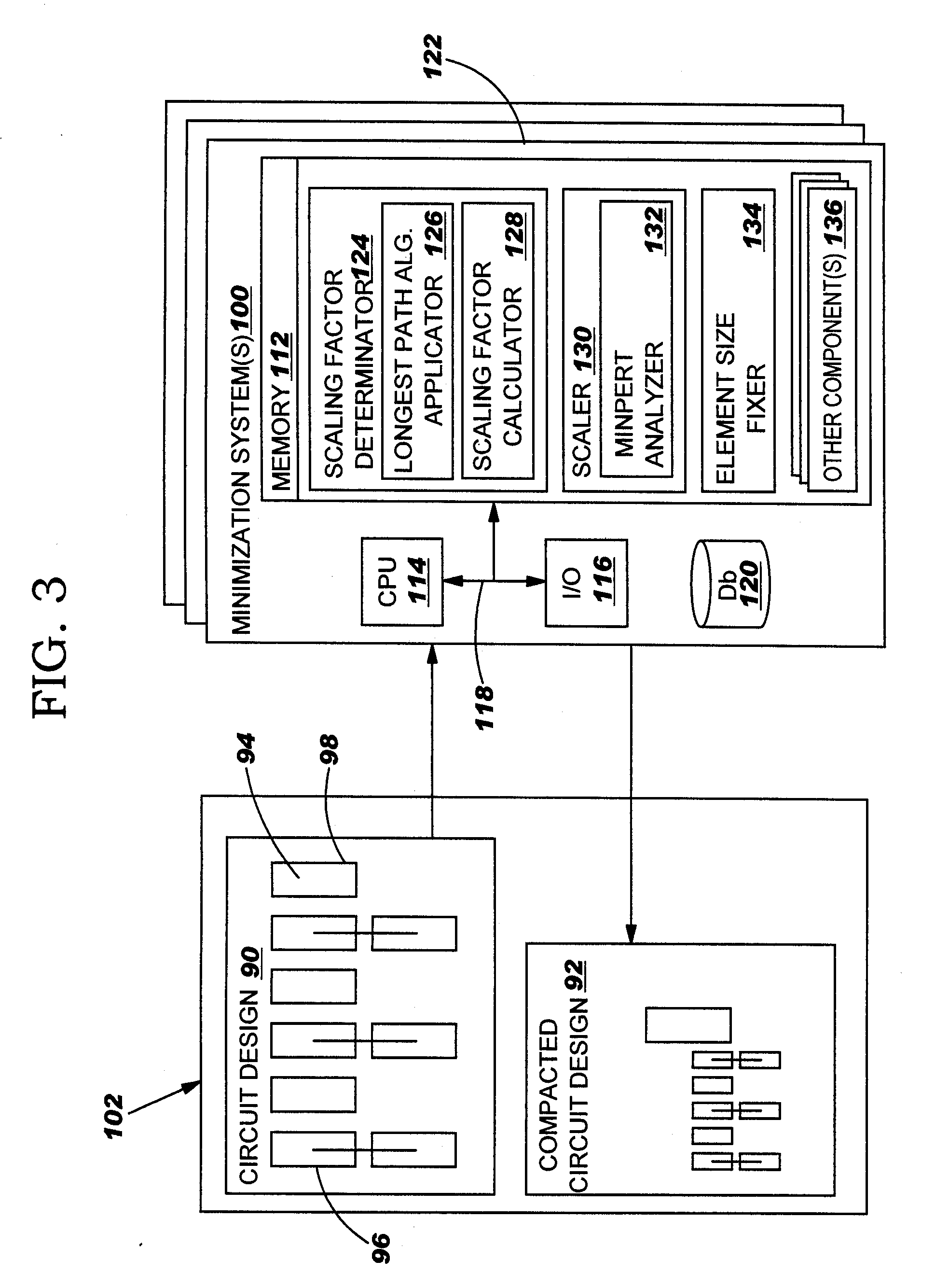
[0025] With reference to the accompanying drawings, FIG. 3 is a block diagram of a circuit design area minimization system 100 (hereinafter “minimization system”) in accordance with the invention. Minimization system 100 includes a memory 112, a central processing unit (CPU) 114, input / output devices (I / O) 116 and a bus 118. A database 120 may also be provided for storage of data relative to processing tasks. Memory 112 includes a program product 122 that, when executed by CPU 114, comprises various functional capabilities described in further detail below. Memory 112 (and database 120) may comprise any known type of data storage system and / or transmission media, including magnetic media, optical media, random access memory (RAM), read only memory (ROM), a data object, etc. Moreover, memory 112 (and database 120) may reside at a single physical location comprising one or more types of data storage, or be distributed across a plurality of physical systems. CPU 114 may likewise compri...


PUM


Abstract

A method, system and program product that implements area minimization of a circuit design while respecting the explicit and implicit design constraints, in the form of ground rules and user intent. A longest path algorithm is used to generate a scaling factor. The scaling factor is used to reduce the size of the circuit design to the minimum legal size. The scaling may be followed by application of minpert analysis to correct any errors introduced by the scaling. The resulting design is shrunk (or expanded) with all elements shrinking (or growing) together by the same factor, and with the relative relationships of elements maintained. In addition, the invention is operational in the presence of a positive cycle, can be run with scaling that freezes the sizes of any structure or ground rule, and can be applied to technology migration.

Description

BACKGROUND OF INVENTION [0001] 1. Technical Field [0002] The present invention relates generally to circuit design, and more particularly, to a method, system and program product for scaling and area minimization of a circuit design. [0003] 2. Related Art [0004] Circuit compaction is an integral part of integrated circuit (IC) chip design methodology for design optimization or migration. In conventional circuit compaction, a circuit design is reduced to its minimum legal size by building a constraint graph that represents the shape edges as nodes, and ground rules and topological relationships as arcs. Each node value represents the edge's current position, and each arc value represents the minimum separation between the edges connected by the arc. In order to illustrate, FIG. 1 shows an illustrative circuit design 8 constraint graph. In a typical circuit compactor, reduction of circuit design 8 is completed by assigning a graph node 10a-d to represent a location of every shape edge...

Claims


Application Information

Patent Timeline
Patent Type & Authority Applications(United States)
IPC IPC(8): G06F17/50H01L21/82
CPCG06F17/5068G06F30/39
Inventor GRAY, MICHAEL S.MCCULLEN, KEVIN W.TELLEZ, GUSTAVO E.WALKER, ROBERT F.
Owner IBM CORP
Why Eureka
Try Eureka