Addressable nanopores and micropores including methods for making and using same

a nanopore and micropore technology, applied in the field of nanopores and micropores, can solve the problems of long nanopores that are not suitable for many applications, can not be produced by many methods, and have a long length of a micrometer or more, and achieve the effect of reducing the diameter of micropores

Active Publication Date: 2005-06-16
BROWN UNIVERSITY +1
View PDF14 Cites 109 Cited by
  • Summary
  • Abstract
  • Description
  • Claims
  • Application Information

AI Technical Summary

Benefits of technology

[0022] The present invention also includes a method for reducing the diameters of micropores to nanometer-scale so as to form nanopores using

Problems solved by technology

Because a freestanding nanometer-thick film is mechanically unstable, the nanopores produced by this technique often have length on the order of a micrometer or more and are typically limited by the thickness of the starting film.
Such long nanopores are not suitable for many applications such as DNA sequencing as currently discussed.
The main drawback of this approach is that highly specialized and expensive ion-beam instrumentation is needed.
This feature is highly undesirable since the DNA molecules will be less likely to access the pore d

Method used


Image

  • Addressable nanopores and micropores including methods for making and using same
  • Addressable nanopores and micropores including methods for making and using same
  • Addressable nanopores and micropores including methods for making and using same

Examples


Embodiment Construction

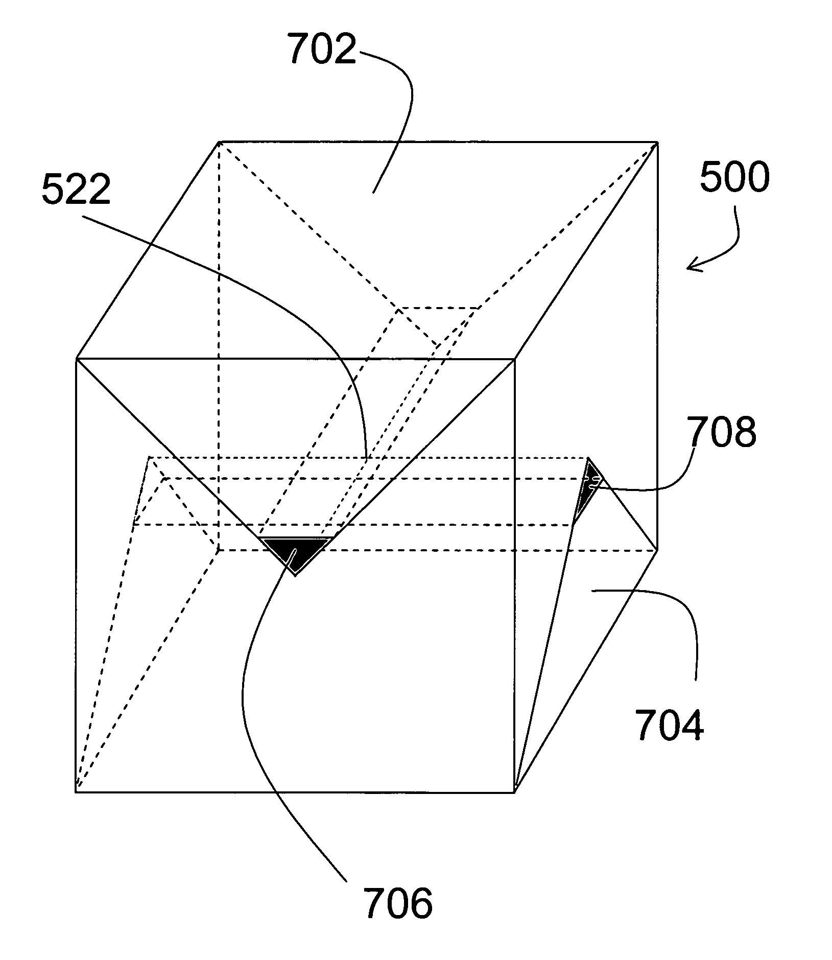
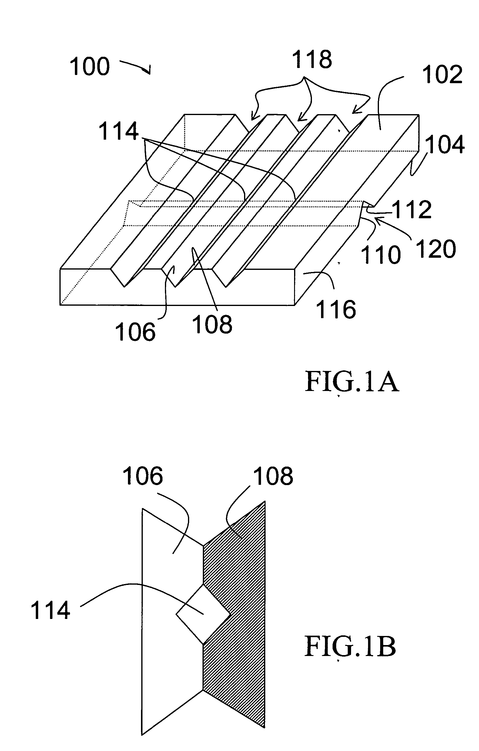
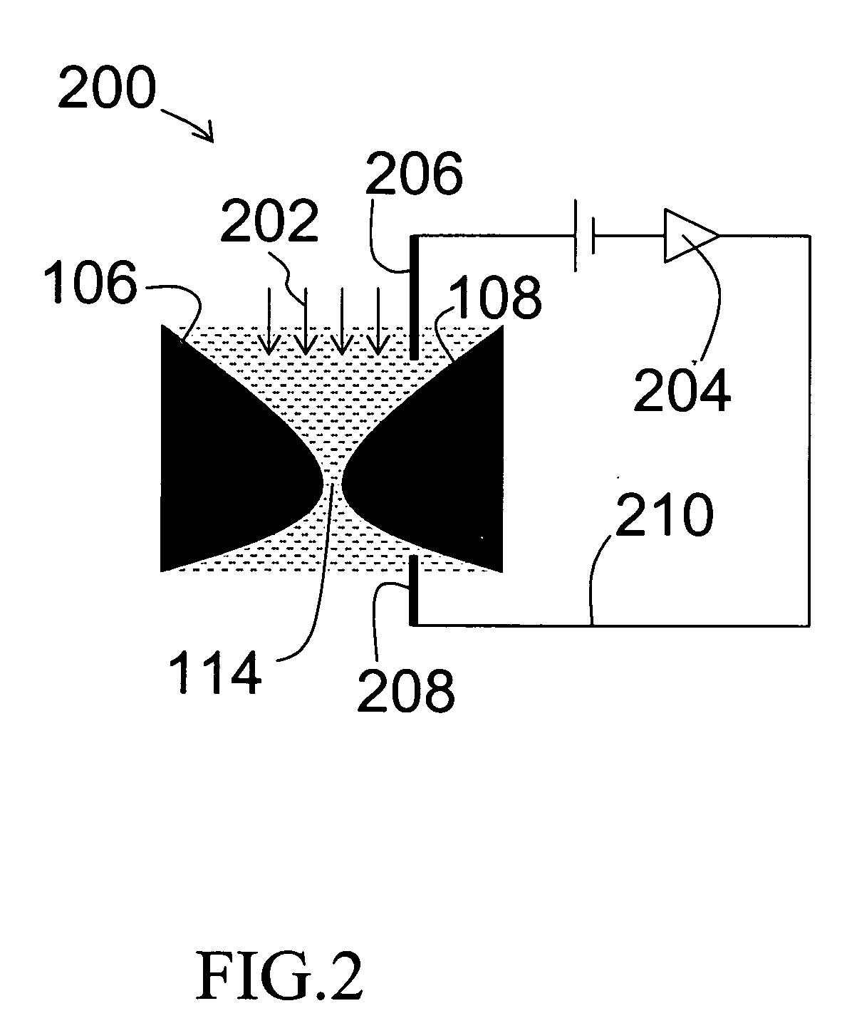
[0036] Referring now to the drawings, a preferred embodiment of the present invention is illustrated in FIG. 1A and FIG. 1B. In FIG. 1A, there is shown a perspective view of device 100 including an array of electrically-addressable nanopores 114, more particularly a linear array of nanopores. The device 100 includes an insulating member 116 having a top surface 102 and a bottom surface 104. A plurality of grooves 118 are formed in the top surface using any of a number of techniques known to those skilled in the art that are appropriate for the material comprising the insulating member. The V-grooves 118 in the top surface 102 are formed in the insulating member 116 so as to generally extend downwardly towards the bottom surface 104 a predetermined distance from the top surface 102. Correspondingly, the V-groove 120 in the bottom surface 104 is formed in the insulating member 116 so as to generally extend upwardly towards the top surface 102 a predetermined distance from the bottom s...


PUM

PropertyMeasurementUnit
Timeaaaaaaaaaa
Widthaaaaaaaaaa
Widthaaaaaaaaaa

Abstract

Featured are devices and systems embodying one or more electrically-addressable-solid-state nanopores useful for sensing and/or characterizing single macromolecules as well as sequencing DNA or RNA. In one aspect of the present invention, there is featured a linear or 2-D electrically-addressable array of nanopores, where the nanopores are located at points of intersections between V-shaped grooves formed in an upper surface of the insulating member and a V-shaped groove formed in a lower surface of the insulating member. In another aspect of the present invention the solid-state nanopore of the present invention the width and/or length of the nanopore is defined or established by sharp edges of cleaved crystals that are maintained in fixed relation during the formation of the insulating member including the nanopore.

Description

CROSS-REFERENCE TO RELATED APPLICATIONS [0001] This application is related to and claims priority from earlier filed Provisional Patent Application No. 60 / 451,088, filed on Feb. 28, 2003; Provisional Patent Application No. 60 / 507,354, filed on Sep. 29, 2003; and Provisional Patent Application No. 60 / 512,140, filed on Oct. 16, 2003.BACKGROUND OF THE INVENTION [0002] The present invention relates generally to nanopore and micropore devices and methods for their manufacture and use. More particularly the present invention relates to nanopore and micropore devices used for detecting, and characterizing biomolecules, as well as sequencing nucleic acids, and new methods for fabrication and application thereof. [0003] Nanopores and micropores are structures that are useful and implemented for a wide range of applications. Nanopores are holes with diameters in the range of 100 nm to 1 nm in a membrane or solid media. Micropores refer to holes with diameters ranging from 100 nm to 100 μm. Fo...

Claims


Application Information

Patent Timeline
IPC IPC(8): B29C47/00B31D3/00C12NC12N1/00C12Q1/68G01N27/26G01N37/00
CPCB82Y5/00B82Y15/00C12Q1/68C12Q1/6869G01N33/48721C12Q1/6874C12Q2565/631Y10S977/932Y10S977/72
Inventor LING, XINSHENG SEAN
Owner BROWN UNIVERSITY
Why Eureka
Try Eureka