Surface-normal optical path structure for infrared photodetection

Active Publication Date: 2005-06-23
MICROSOFT TECH LICENSING LLC
View PDF7 Cites 47 Cited by
  • Summary
  • Abstract
  • Description
  • Claims
  • Application Information

AI Technical Summary

Benefits of technology

[0012] The present invention SiGe optical path structure (absorbs IR wavelength light that is normal to a silicon substrate surface and parallel to the SiGe/Si heterojunction interface, increasing the length of the optical path. Therefore, a two-dimensional IR image detection can be realized with a thin SiGe thickness. Because of the relatively poor quantum efficiencies associated with SiGe, the IR absorption length of SiGe must be long, and conventionally a thick SiGe layer is needed to absorb high amounts of IR energy.

Problems solved by technology

However, it is very difficult to grow defect-free thick SiGe film on Si

Method used


Image

  • Surface-normal optical path structure for infrared photodetection
  • Surface-normal optical path structure for infrared photodetection
  • Surface-normal optical path structure for infrared photodetection

Examples


Embodiment Construction

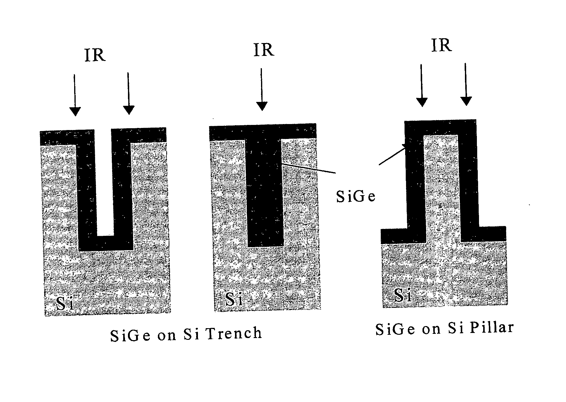
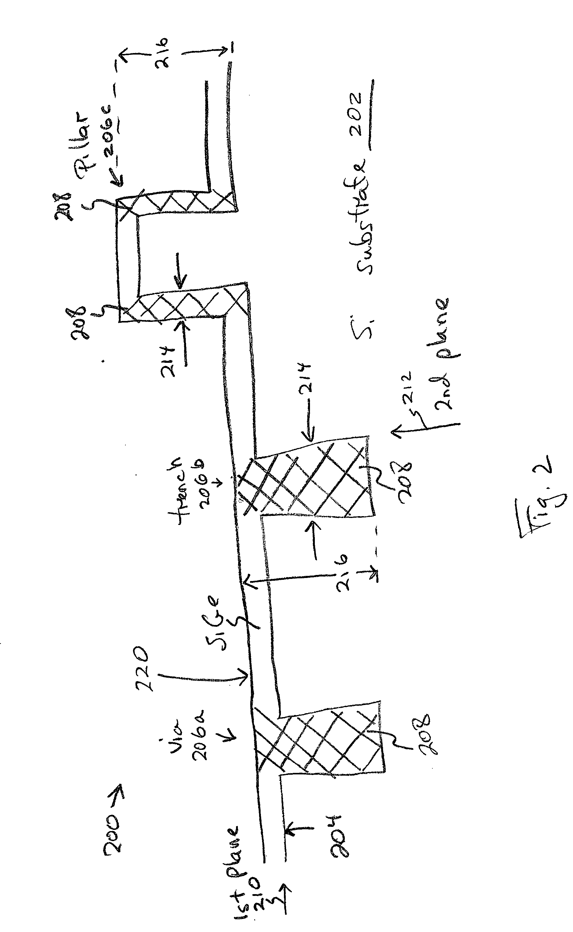
[0034]FIG. 2 is a cross-sectional view of the present invention SiGe optical path structure, normal to a Si substrate surface, for IR photodetection. The structure 200 comprises a Si substrate 202 with a surface 204. A Si feature 206 is normal with respect to the Si substrate surface 204. As shown, the feature 206 can be a via 206a, a trench 206b, or a pillar 206c. A surface-normal SiGe optical path 208, shown with double cross-hatched lines, overlies the Si feature 206.

[0035] The Si substrate surface (interface) 204 is formed in a first plane 210 parallel to the substrate surface 204. SiGe is epitaxially grown on the Si surface 204 and Si feature 206. The surface-normal SiGe optical path 208 is formed in a second plane 212, normal to the first plane 210. That is, the optical path 208 is normal to the substrate surface 204. Alternately stated, the feature 206 has an element or structure in a vertical plane that is perpendicular to the horizontal surface 204. Note, that the feature ...


PUM


Abstract

A SiGe surface-normal optical path photodetector structure and a method for forming the SiGe optical path normal structure are provided. The method comprises: forming a Si substrate with a surface; forming a Si feature, normal with respect to the Si substrate surface, such as a via, trench, or pillar; depositing SiGe overlying the Si normal feature to a thickness in the range of 5 to 1000 nanometers (nm); and, forming a SiGe optical path normal structure having an optical path length in the range of 0.1 to 10 microns. Typically, the SiGe has a Ge concentration in the range from 5 to 100%. The Ge concentration may be graded to increase with respect to the deposition thickness. For example, the SiGe may have a 20% concentration of Ge at the Si substrate interface, a 30% concentration of Ge at a SiGe film top surface, and a thickness of 400 nm.

Description

BACKGROUND OF THE INVENTION [0001] 1. Field of the Invention [0002] This invention generally relates to integrated circuit (IC) fabrication processes and, more particularly, to a surface-normal infrared optical path structure and corresponding fabrication method. [0003] 2. Description of the Related Art [0004] There are many applications for photodetection in the near infrared region (the wavelength between 0.7 micron to 2 microns), such as in fiber-optical communication, security, and thermal imaging. Although III-V compound semiconductors provide superior optical performance over their silicon (Si)-based counterparts, the use of Si is desirable, as the compatibility of Si-based materials with conventional Si-IC technology promises the possibility of cheap, small, and highly integrated optical systems. [0005] Silicon photodiodes are widely used as photodetectors in the visible light wavelengths due to their low dark current and the above-mentioned compatibility with Si IC technolog...

Claims


Application Information

Patent Timeline
IPC IPC(8): G01J5/20H01L21/00H01L21/20H01L27/146H01L29/165H01L31/028H01L31/0352H01L31/10H01L31/109H01L31/18
CPCH01L21/02381Y02E10/547H01L21/0245H01L21/02532H01L21/02639H01L27/14627H01L27/14643H01L31/0232H01L31/028H01L31/035281H01L31/105H01L31/108H01L31/109H01L31/1812H01L21/0243H01L31/02327
Inventor LEE, JONG JANMAA, JER-SHENTWEET, DOUGLAS J.HSU, SHENG TENG
Owner MICROSOFT TECH LICENSING LLC
Why Eureka
Try Eureka