Semiconductor structure with metal migration semiconductor barrier layers and method of forming the same

a technology of semiconductor barrier layer and semiconductor structure, which is applied in the direction of semiconductor device, semiconductor/solid-state device details, electrical apparatus, etc., can solve the problems of structure failure, prior art approach may still be susceptible to metal diffusion, etc., to improve the high temperature reliability and performance time, and improve the stability of the semiconductor structur

Active Publication Date: 2005-06-23
THE BOEING CO
View PDF4 Cites 3 Cited by
  • Summary
  • Abstract
  • Description
  • Claims
  • Application Information

AI Technical Summary

Benefits of technology

[0010] The present invention provides a semiconductor structure that has one or more metal migration semiconductor barrier layers incorporated within or outside of a semiconductor contact layer and, therefore, provides a contact structure with improved high temperature reliability. The present invention further provides a semiconductor structure that is suitable for, but not limited to, use in multifunction solar cells that provide power to spacecraft, for example, satellites. The present invention still further provides an appropriate semiconductor material, such as AlInP, that may be incorporated within the contact structure of a semiconductor structure and that prevents metal protrusion from the metal contact into the semiconductor active layers during long-term exposure of the semiconductor structure to high temperatures, improving the performance, high temperature reliability, and stability of the semiconductor structure. The present invention still further provides a method for forming a semiconductor structure with metal migration semiconductor barrier layers and therefore, for improving the high temperature reliability and the performance time at high temperatures of the semiconductor structure.

Problems solved by technology

However, this prior art approach may still be susceptible to metal diffusion under certain environmental conditions, such as exposure of the semiconductor structure to high temperatures for prolonged periods of time.
Consequently, it will be only a matter of time until the metal reaches the semiconductor active layers 11 and causes the structure to fail.

Method used


Image

  • Semiconductor structure with metal migration semiconductor barrier layers and method of forming the same
  • Semiconductor structure with metal migration semiconductor barrier layers and method of forming the same
  • Semiconductor structure with metal migration semiconductor barrier layers and method of forming the same

Examples


Embodiment Construction

[0029] The following detailed description is of the best currently contemplated modes of carrying out the invention. The description is not to be taken in a limiting sense, but is made merely for the purpose of illustrating the general principles of the invention, since the scope of the invention is best defined by the appended claims.

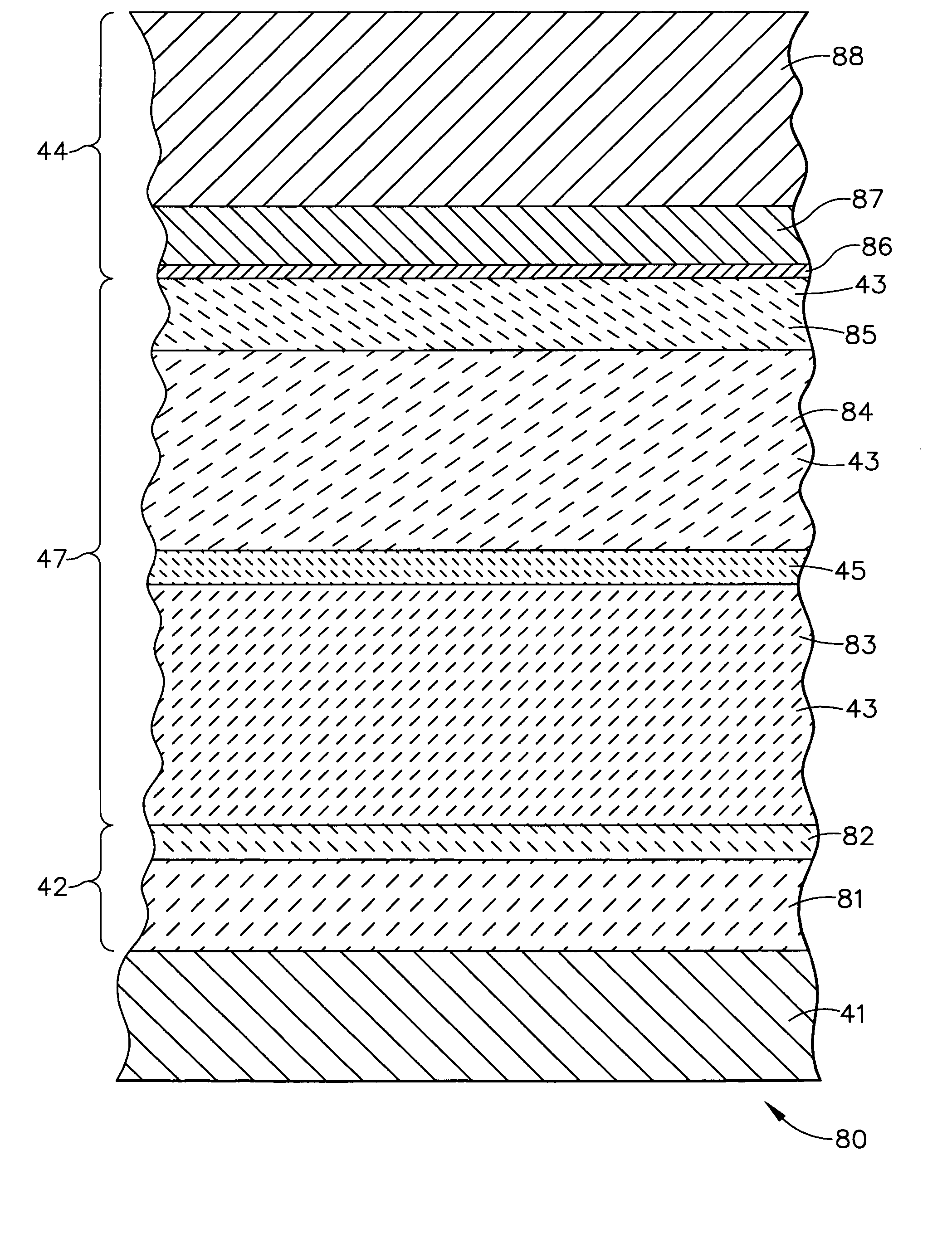
[0030] Broadly, an embodiment of the present invention provides a semiconductor structure with a contact structure for improved high temperature reliability. Contrary to the known prior art, the contact structure may include one or more metal migration semiconductor barrier layers embedded within or in intimate contact with a semiconductor contact layer that may be designed to block the movement of metal from the metal contact towards the semiconductor active region. The semiconductor structure as in one embodiment of the present invention may be used, for example, for III-V based multifunction solar cells that provide power to spacecraft, such as sat...


PUM


Abstract

A semiconductor structure includes a semiconductor substrate, a semiconductor active region, a semiconductor contact layer, at least one metal migration semiconductor barrier layer, and a metal contact. The metal migration semiconductor barrier layer may be embedded within the semiconductor contact layer. Furthermore, the metal migration semiconductor barrier layer may be located underneath or above and in intimate contact with the semiconductor contact layer. The metal migration semiconductor barrier layer and the semiconductor contact layer form a contact structure that prevents metals from migrating from the metal contact into the semiconductor active layer during long-term exposure to high temperatures. By providing a robust contact structure that may be used in semiconductor structures, for example in solar cells that power spacecraft or terrestrial solar cells used under concentrated sunlight, the high temperature reliability of the semiconductor structure will be improved and the operation time will be prolonged.

Description

BACKGROUND OF THE INVENTION [0001] The present invention generally relates to semiconductor structures and, more particularly, to semiconductor structures including metal migration barrier layers preventing metal migration from a contact layer into an active layer of a semiconductor structure and method of forming the same. [0002] While manufacturing semiconductor devices, such as III-V semiconductor based multifunction solar cells, electrical contacts are formed on individual semiconductor devices and connected together to perform the desired circuit functions. The electrical contact formation and connection process involves metal layers and is generally called “metallization”. Metal contact layers containing multiple thin layers with alternating composition of, for example Ti / Au / Ag, are conventionally used for providing electrical contact to semiconductor devices. [0003]FIG. 1 provides a schematic cross sectional view of a typical prior art semiconductor structure 10. The semicond...

Claims


Application Information

Patent Timeline
Patent Type & Authority Applications(United States)
IPC IPC(8): H01L23/48
CPCH01L31/022425H01L31/0304Y02E10/547Y02E10/544H01L31/068
Inventor YOON, HOJUNKING, RICHARDKUKULKA, JERRY R.ERMER, JAMES H.LAU, MAGGY L.
Owner THE BOEING CO
Why Eureka
Try Eureka