Processing unit having a dual channel bus architecture

a processing unit and bus architecture technology, applied in the field of data processing, can solve the problems of significant drawbacks, delay in sending input data to all pus, and limitations of existing hardware solutions, so as to improve performance and scalability, and increase the circuit complexity of pus

Inactive Publication Date: 2005-06-23
IBM CORP
View PDF3 Cites 8 Cited by
  • Summary
  • Abstract
  • Description
  • Claims
  • Application Information

AI Technical Summary

Benefits of technology

[0015] The present invention addresses the above-described need by providing a processing unit having a dual channel bus architecture that allows improved performance and scalability. This architecture permits considerable expansion of the number of PUs without requiring a significant increase in circuit wiring and without any degradation in processing speed. At the cost of a very slightly increasing the circuit complexity of PUs, the need for external circuitry to merge a considerable number of PUs together is avoided.
[0016] In addition, the processing unit of the present invention permits a reduction in the amount of re-drive devices necessary to distribute the input data and to collect the output data, i.e. the results.
[0017] Furthermore, the architecture of the processing unit of the present invention permits a regular circuit floor planning placement at the chip and card level; reduces power dissipation; and allows a total pipelined operation.
[0019] With this architecture, scaling is accomplished by increasing the number of IPUs without increasing system complexity. Increasing the number of IPUs requires only local connections without requiring additional circuitry outside the IPUs.

Problems solved by technology

For real-time applications, existing hardware solutions have some major limitations concerning scalability and input / output bandwidth.
The first cause of these limitations is due to the wiring.
If, as illustrated in FIG. 1, the results output by the PUs were directly applied on the output bus, this implementation would be operative but would still have some significant drawbacks when the number of PUs further increases.
In particular, the delay to send the input data to all PUs would be very important.
The implementation depicted in FIG. 2 results in large delays on the output bus, caused by the trees forming blocks 20 and 22, and therefore reduced output time.
Moreover, it is to be noted that said trees in blocks 20 and 22 also increase the area needed to implement such an architecture in hardware which in turn, reduce the processing speed and limit the scalability.
On the other hand, a performance limitation is due to some data contention that can occur on the input and output buses.
But the most important data contention occurs on the output bus during the comparison phase.
When the comparison is completed, it is necessary to know all distances between the input pattern and the reference patterns stored in the PUs, and because, all PUs are using the same output bus to send the result, the outputting phase can take a long time.
Consequently, as apparent in FIG. 3, because the output delay time takes more than one clock cycle, the output bus is busy most of the time.
It does also exist a limitation directly related to the scaling capability.
The above problem related to card 33 design, is also present for the ASIC chip 25 design, as it is sometimes difficult to make an efficient floor planning placement, and the wiring is complex due to the many global signals that are distributed to all PUs.

Method used


Image

  • Processing unit having a dual channel bus architecture
  • Processing unit having a dual channel bus architecture
  • Processing unit having a dual channel bus architecture

Examples


Embodiment Construction

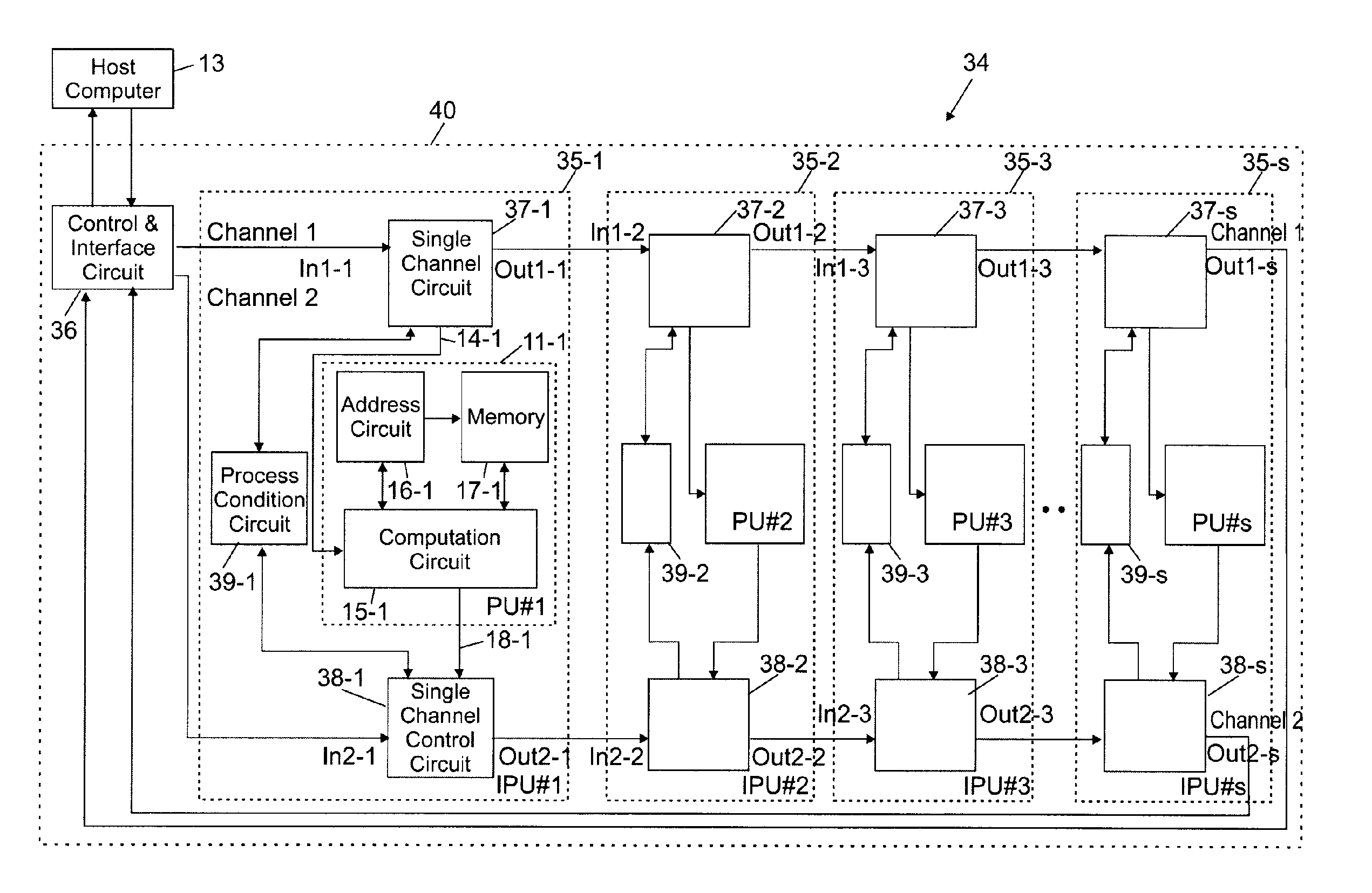
[0037]FIG. 5A shows a system comprised of a plurality of improved processing units (IPUs) having a dual channel bus architecture according to the present invention. FIG. 5B shows a variant of the FIG. 5A system. Now turning to FIG. 5A, the system referenced 34 includes a number s of IPUs, referenced 35-1 to 35-s, a control & interface circuit (CI) circuit now referenced 36 because it can have a structure slightly different of the conventional CI circuits 12 and 12′ previously shown, and the host computer 13 as standard. Each IPU is organized around the conventional PU (generically referenced 11 in FIGS. 1 and 2) and further includes a pair of single channel control (SCC) circuits and a process condition (PC) circuit. Let us consider IPU 35-2 for the sake of illustration. The upper SCC circuit 37-2 has a serial connection with the corresponding SCC circuits 37-1 and 37-3 of the previous and next IPUs 35-1 and 35-3. This type of connection applies to each IPU, except for the first IPU...


PUM


Abstract

A processing unit having a dual channel bus architecture associated with a specific instruction set, configured to receive an input message and transmit an output message that is identical or derived therefrom. A message consists of one opcode, with or without associated data, used to control each processing unit depending on logic conditions stored in dedicated registers in each unit. Processing units are serially connected but can work simultaneously for a total pipelined operation. This dual architecture is organized around two channels labeled Channel 1 and Channel 2. Channel 1 mainly transmits an input message to all units while Channel 2 mainly transmits the results after processing in a unit as an output message. Depending on the logic conditions, an input message not processed in a processing unit may be transmitted to the next one without any change.

Description

FIELD OF THE INVENTION [0001] The present invention relates to data processing, and more particularly to an improved processing unit having a dual channel bus architecture that allows a serial transmission of data from a host computer to a very large number of such processing units and their parallel processing for a totally pipelined operation. The present invention can find extensive applications in pattern recognition systems. BACKGROUND OF THE INVENTION [0002] To recognize specific patterns within a set of data is important in many fields, including speech and pattern recognition, image processing, seismic data analysis, etc.. If the real-time data processing is too intensive for one processing unit (PU), then several PUs can be used in parallel to increase the computational power. For real-time applications, existing hardware solutions have some major limitations concerning scalability and input / output bandwidth. For instance, in the field of pattern recognition, a typical appl...

Claims


Application Information

Patent Timeline
Patent Type & Authority Applications(United States)
IPC IPC(8): G06F15/00G06F15/173
CPCG06F15/17368
Inventor TANNHOF, PASCALSLYFIELD, JAN
Owner IBM CORP
Why Eureka
Try Eureka