Multi-chip module with third dimension interconnect

a technology of multi-chip modules and interconnections, applied in the direction of multi-programming arrangements, instruments, and architectures with multiple processing units, can solve the problems of complex programming techniques, complex programming techniques, and heterogeneous combination of computers and computing devices on today's computer network, so as to avoid the computational overhead of a data synchronization scheme implemented

Inactive Publication Date: 2005-06-23
IBM CORP
View PDF4 Cites 36 Cited by
  • Summary
  • Abstract
  • Description
  • Claims
  • Application Information

AI Technical Summary

Benefits of technology

[0015] In accordance with the present invention, all members of a computer network, i.e., all computers and computing devices of the network, are constructed from a common computing module. This common computing module has a consistent structure and preferably employs the same ISA. The members of the network can be, e.g., clients, servers, PCs, mobile computers, game machines, PDAs, set top boxes, appliances, digital televisions and other devices using computer processors. The consistent modular structure enables efficient, high speed processing of applications and data by the network's members and the rapid transmission of applications and data over the network. This structure also simplifies the building of members of the network of various sizes and processing power and the preparation of applications for processing by these members.
[0020] In another aspect, the present invention provides a synchronized system and method for an APU's reading of data from, and the writing of data to, the shared DRAM. This system avoids conflicts among the multiple APUs and multiple PEs sharing the DRAM. In accordance with this system and method, an area of the DRAM is designated for storing a plurality of full-empty bits. Each of these full-empty bits corresponds to a designated area of the DRAM. The synchronized system is integrated into the hardware of the DRAM and, therefore, avoids the computational overhead of a data synchronization scheme implemented in software.
[0021] The present invention also implements sandboxes within the DRAM to provide security against the corruption of data for a program being processed by one APU from data for a program being processed by another APU. Each sandbox defines an area of the shared DRAM beyond which a particular APU, or set of APUs, cannot read or write data.
[0024] In another aspect, the present invention provides an absolute timer for the processing of tasks. This absolute timer is independent of the frequency of the clocks employed by the APUs for the processing of applications and data. Applications are written based upon the time period for tasks defined by the absolute timer. If the frequency of the clocks employed by the APUs increases because of, e.g., enhancements to the APUs, the time period for a given task as defined by the absolute timer remains the same. This scheme enables the implementation of enhanced processing times by newer versions of the APUs without disabling these newer APUs from processing older applications written for the slower processing times of older APUs.

Problems solved by technology

This heterogeneous combination of computers and computing devices on today's computer networks complicates the processing and sharing of data and applications.
The sharing of data and applications among this assortment of computers and computing devices presents substantial problems.
These techniques include, among others, sophisticated interfaces and complicated programming techniques.
These solutions often require substantial increases in processing power to implement.
They also often result in a substantial increase in the time required to process applications and to transmit data over networks.
While this approach minimizes the amount of bandwidth needed, it also often causes frustration among users.
This additional layer of software significantly degrades a processor's processing speed.
These viruses and malfunctions can corrupt a client's database and cause other damage.
Although a security protocol employed in the Java model attempts to overcome this problem by implementing a software “sandbox,” i.e., a space in the client's memory beyond which the Java applet cannot write data, this software-driven security model is often insecure in its implementation and requires even more processing.
These network applications require extremely fast processing speeds.
The current architecture of networks, and particularly that of the Internet, and the programming model presently embodied in, e.g., the Java model, make reaching such processing speeds extremely difficult.

Method used


Image

  • Multi-chip module with third dimension interconnect
  • Multi-chip module with third dimension interconnect
  • Multi-chip module with third dimension interconnect

Examples


Embodiment Construction

[0060] The following is intended to provide a detailed description of an example of the invention and should not be taken to be limiting of the invention itself. Rather, any number of variations may fall within the scope of the invention, which is defined in the claims following the description.

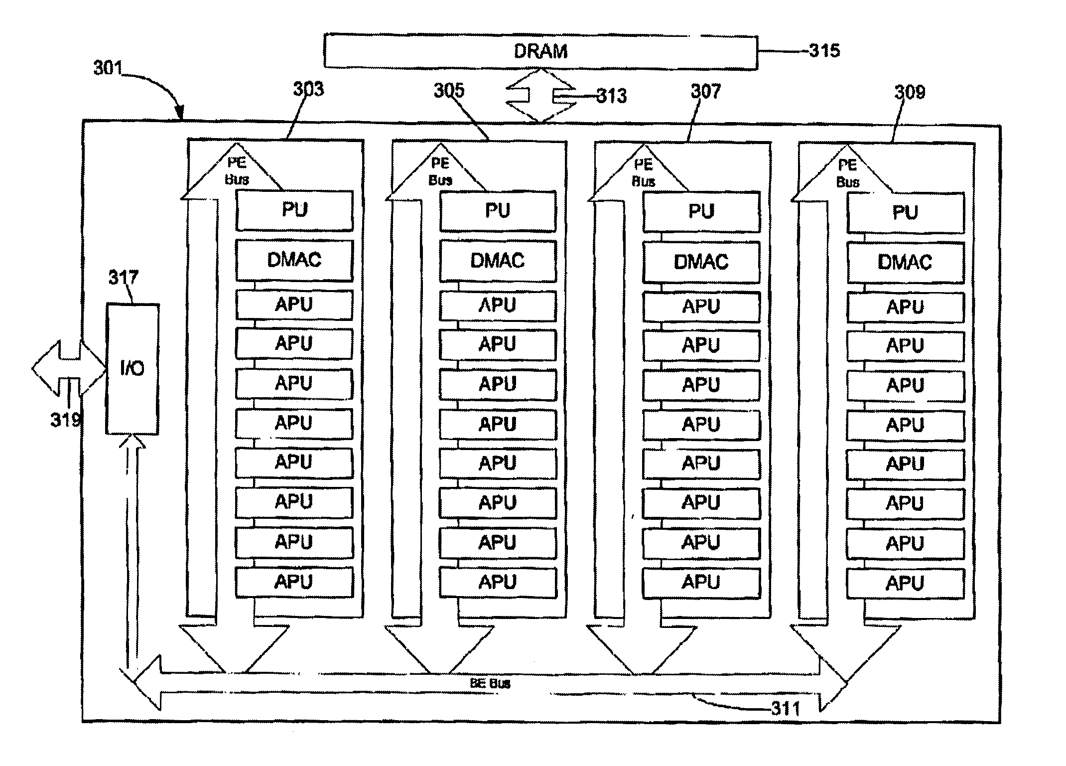
[0061] The overall architecture for a computer system 101 in accordance with the present invention is shown in FIG. 1.

[0062] As illustrated in this figure, system 101 includes network 104 to which is connected a plurality of computers and computing devices. Network 104 can be a LAN, a global network, such as the Internet, or any other computer network.

[0063] The computers and computing devices connected to network 104 (the network's “members”) include, e.g., client computers 106, server computers 108, personal digital assistants (PDAs) 110, digital television (DTV) 112 and other wired or wireless computers and computing devices. The processors employed by the members of network 104 are con...


PUM


Abstract

A computer architecture and programming model for high speed processing over broadband networks are provided. The architecture employs a consistent modular structure, a common computing module and uniform software cells. The common computing module includes a control processor, a plurality of processing units, a plurality of local memories from which the processing units process programs, a direct memory access controller and a shared main memory. A synchronized system and method for the coordinated reading and writing of data to and from the shared main memory by the processing units also are provided. A hardware sandbox structure is provided for security against the corruption of data among the programs being processed by the processing units. The uniform software cells contain both data and applications and are structured for processing by any of the processors of the network. Each software cell is uniquely identified on the network.

Description

1. RELATED APPLICATIONS [0001] This application is a Continuation of U.S. patent application U.S. 2002 / 0138637 A1 filed on Mar. 22, 2001 titled “Computer Architecture and Software Cells for Broadband Networks,” and has at least one of the same inventors as the above referenced U.S. patent application.BACKGROUND OF THE INVENTION [0002] 1. Technical Field [0003] The present invention relates in general to a multi-chip module with third dimension interconnect. More particularly, the present invention relates to one or more processor modules that includes one or more first buses in a first dimension and a memory module that couples to the processor modules using a third dimension interconnect and also includes one or more second buses in a second dimension. [0004] 2. Description of the Related Art [0005] The present invention relates to an architecture for computer processors and computer networks and, in particular, to an architecture for computer processors and computer networks in a ...

Claims


Application Information

Patent Timeline
Patent Type & Authority Applications(United States)
IPC IPC(8): G06F9/44G06F9/50G06F15/177G06F15/16G06F15/80H04L29/06H04L29/08
CPCG06F9/4862G06F15/16H04L67/10H04L63/168H04L67/34H04L29/06027G06F9/30061H04L65/1101
Inventor HOFSTEE, HARM PETERJOHNS, CHARLES RAYKAHLE, JAMES ALLAN
Owner IBM CORP
Why Eureka
Try Eureka