Signal routing in a hermetically sealed MEMS device

Active Publication Date: 2005-06-30
HONEYWELL INT INC
View PDF18 Cites 27 Cited by
  • Summary
  • Abstract
  • Description
  • Claims
  • Application Information

AI Technical Summary

Benefits of technology

[0024] According to another aspect of the invention, the present invention overcomes the limitations of the prior art by providing a method of forming a hermetically sealed MEMS device, the method includes, in an epitaxial layer of semiconductor silicon, forming each of a micro-machined electromechanical device, a pillar physically separated from the micro-machined electromechanical device, and a seal ring surrounding the micro-machined electromechanical device and the pillar. The also method includes forming in one or more glass substrates one or more cover plates having an internal surface structured to cooperate with the micro-machined electromechanical device and having a peripheral surface structured for joining to the seal ring, one of the cover plates being formed with a window that communicates between an inner surface and an outer surface of the cover plate.
[0025] Furthermore, the method includes anodically bondin

Problems solved by technology

Moving parts within a device are typically separated by microscopically narrow critical gap spacings, and as such are highly sensitive to particle contamination, such as dust and other microscopic debris.
MEMS devices are also sensitive to contamination arising from corrosive environments; humidity and H2O in either the liquid or vapor phase, which may cause stiction problems in the finished device; and mechanical damage such as abrasion.
Each of the individual processes may expose the device to a source of contamination.
This sensitivity to particle contamination poses a challenge to the structural design and microfabrication processes ass

Method used


Image

  • Signal routing in a hermetically sealed MEMS device
  • Signal routing in a hermetically sealed MEMS device
  • Signal routing in a hermetically sealed MEMS device

Examples


Embodiment Construction

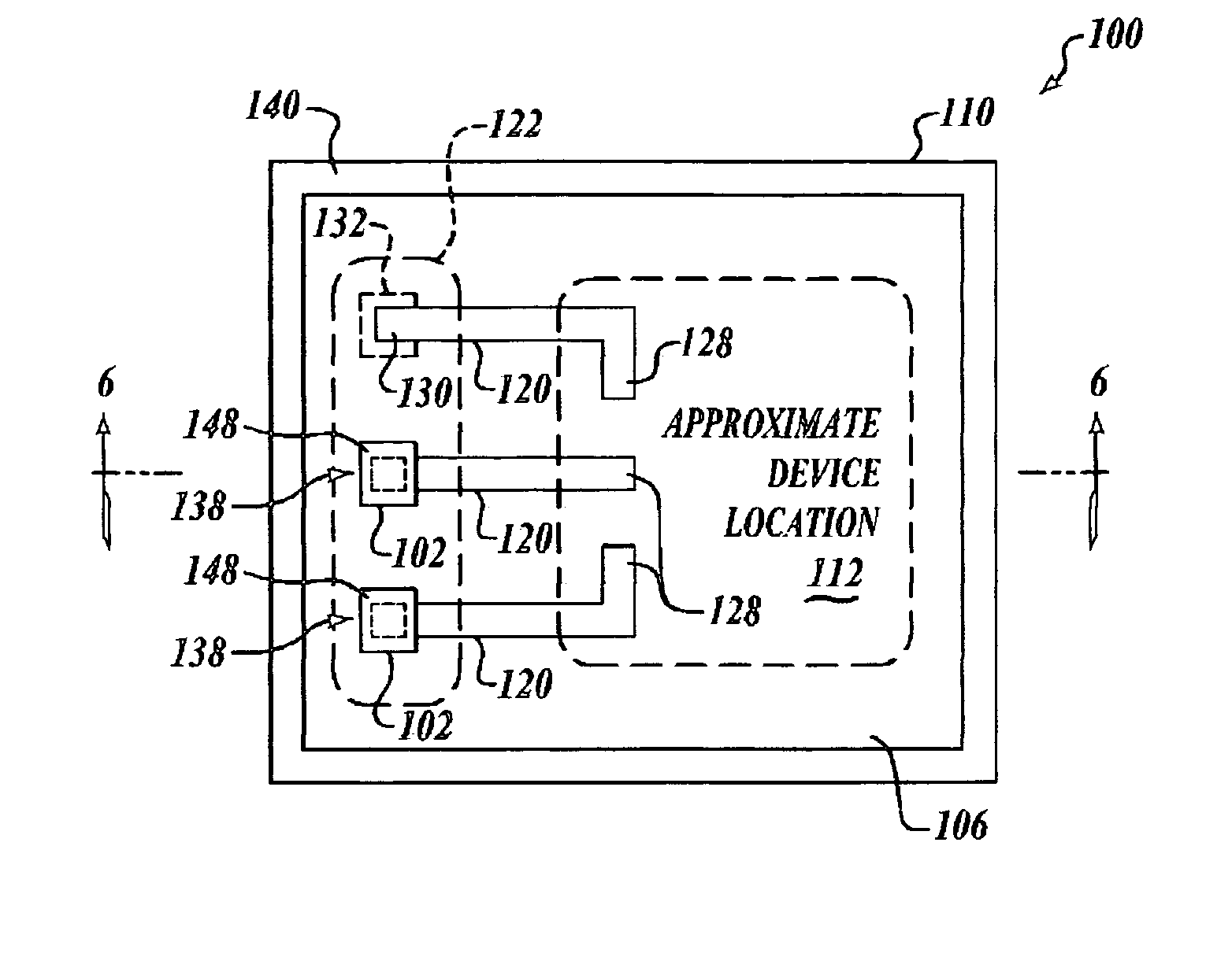
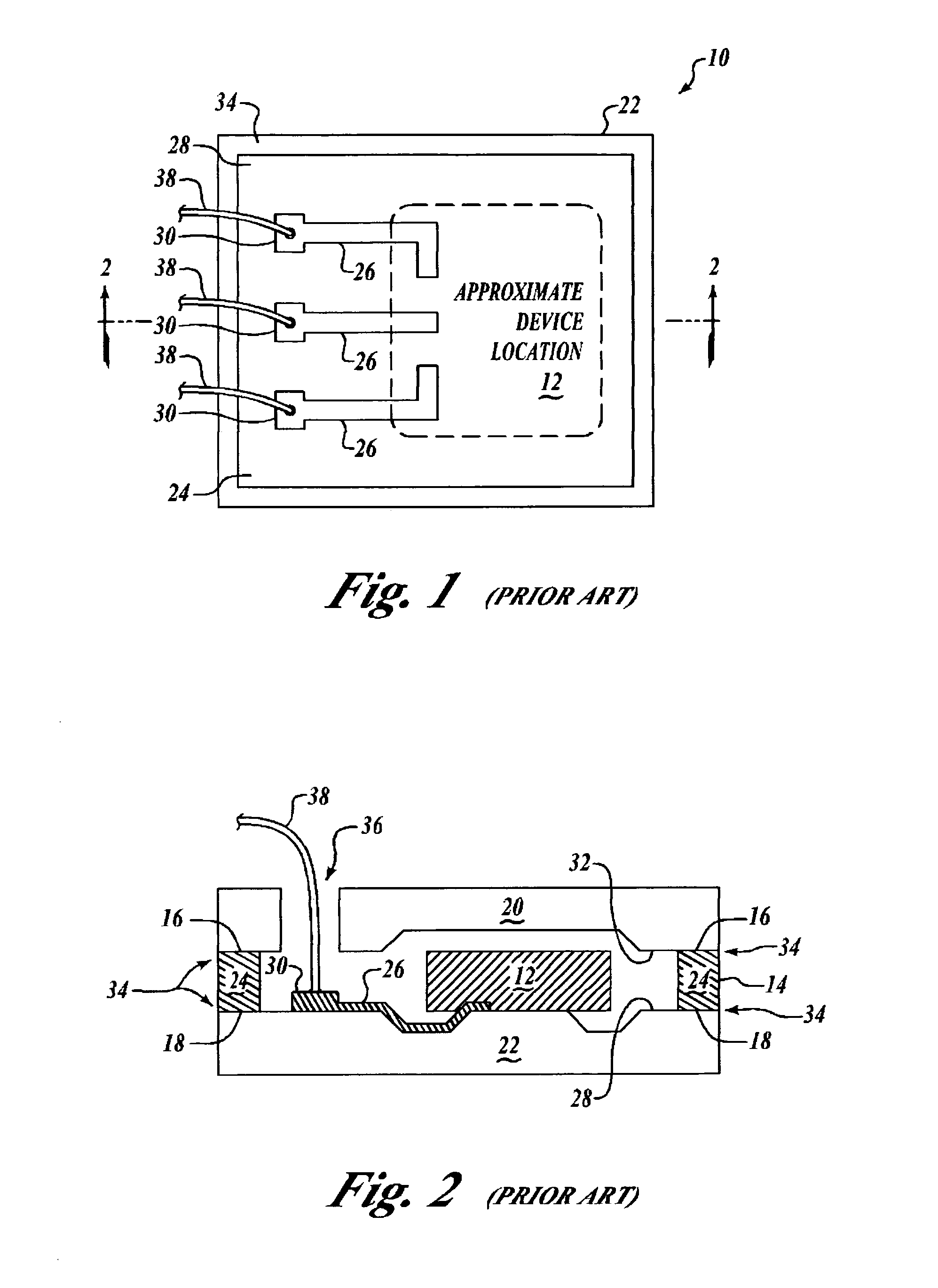
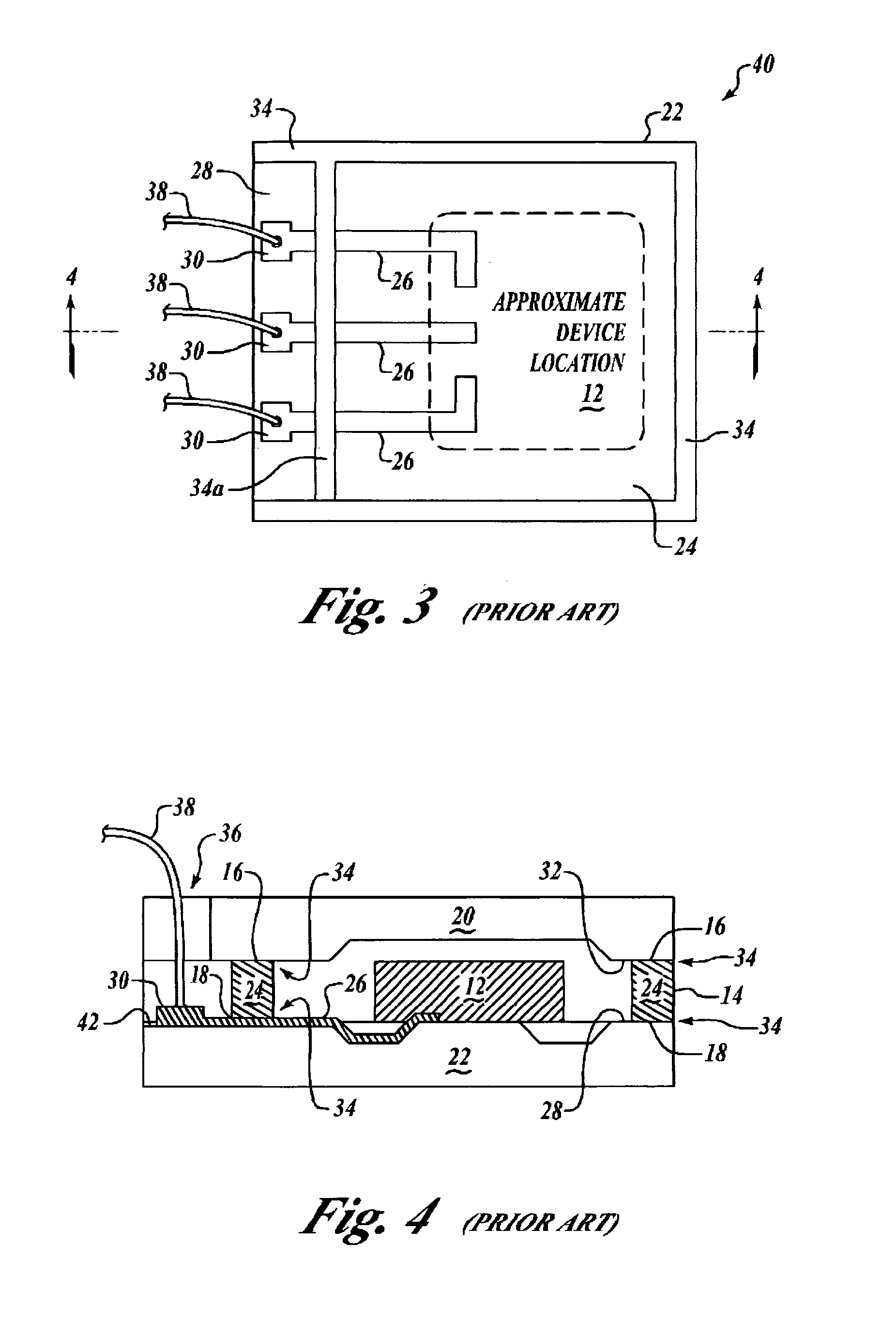
[0037] In the Figures, like numerals indicate like elements.

[0038] The present invention is an apparatus and method for using wide columns of anodically bonded semiconductor silicon to route signals by conductive paths to a plurality of wire bond pads that are located external to the hermetic seal of hermetically sealed micro-machined electromechanical system (MEMS) devices and methods for manufacturing the same. Accordingly, the apparatus and method of the invention are realized in a hermetically sealed MEMS device having a micro-machined electromechanical device formed of semiconductor silicon and a pair of spaced apart top and bottom cover plates, the cover plates being made either of respective Pyrex RTM glass wafers or of silicon substrates having thin glass inner surfaces deposited thereon of a type that are known to be suitable for forming anodic silicon-to-glass bonds. The cover plates having their inner glass surfaces structured to cooperate with the micro-machined electro...


PUM


Abstract

A hermetically sealed MEMS device having a micro-machined electromechanical device, a plurality of pillars at spaced-apart positions removed from the micro-machined electromechanical device, and a peripheral seal ring completely surrounding both the micro-machined electromechanical device and the pillars, all patterned in a layer of epitaxial semiconductor silicon. A glass cover is structured to cooperate with the micro-machined electromechanical device and is sealed by the seal ring. A plurality of pass-through windows are formed internal of the cover and communicate between inner and outer surfaces of the cover. Each of the pillars covers one of the windows. A plurality of internal electrical conductors electrically couple the micro-machined electromechanical device with a surface of each of the pillars.

Description

FIELD OF THE INVENTION [0001] The present invention relates generally to devices fabricated as micro-machined electromechanical system (MEMS) devices and methods for manufacturing the same, and in particular to hermetically sealed MEMS devices and methods for routing signals into and out of MEMS devices. BACKGROUND OF THE INVENTION [0002] Many devices fabricated as micro-machined electromechanical systems (MEMS), both sensor and actuator devices, and methods for manufacturing the same are generally well-known. See, for example, U.S. patent application Ser. No. 09 / 963,142, METHOD OF TRIMMING MICRO-MACHINED ELECTROMECHANICAL SENSORS (MEMS) DEVICES, filed in the name of Paul W. Dwyer on Sep. 24, 2001, which is assigned to the assignee of the present application and the complete disclosure of which is incorporated herein by reference, that describes a MEMS acceleration sensor and method for manufacturing the same. In another example, U.S. Pat. No. 6,428,713, MEMS SENSOR STRUCTURE AND MI...

Claims


Application Information

Patent Timeline
IPC IPC(8): B81B7/00H01L23/552H01L29/84
CPCB81C2203/0118B81B7/007H01L2224/48091H01L2924/00014
Inventor ESKRIDGE, MARK H.COUSSEAU, PETER
Owner HONEYWELL INT INC
Why Eureka
Try Eureka