
High-frequency device

a high-frequency device and conductive post technology, applied in semiconductor devices, semiconductor/solid-state device details, electrical apparatus, etc., can solve the problems of serious deformation of high-frequency signal characteristics and rather large height of electrically conductive posts formed in resin layers, and achieve the effect of reducing size and improving high-frequency characteristics

Active Publication Date: 2005-06-30
FUJITSU LTD
View PDF0 Cites 20 Cited by
  • Summary
  • Abstract
  • Description
  • Claims
  • Application Information

AI Technical Summary

Benefits of technology

The present invention provides a high-frequency device that has a smaller size and improved high-frequency characteristic by using a chip sized package and optimizing the size and arrangement of electrically conductive pads and posts. The invention also includes a configuration with a first shielding layer to reduce parasitic capacitance and resistance, and an inductor for impedance matching. Additionally, the invention provides a high-frequency device module that can process signals of different high-frequency bands with different electrically conductive posts. The invention also addresses the issue of degraded high-frequency characteristic due to the size of the electrically conductive posts.

Problems solved by technology

However, the sealing electrically insulating layer or resin layer having a sealing function are much thicker than the multilayer wiring layers on the chip surface, the height of the electrically conductive posts formed in the resin layer becomes rather large, and the characteristics relating to high-frequency signals are seriously degraded.

Method used


Image

  • High-frequency device
  • High-frequency device
  • High-frequency device

Examples


Embodiment Construction

[0054] Embodiments of the present invention will be described below with reference to the appended drawings. However, the scope of the present invention is not limited to those embodiments and covers the inventions described in the patent claims and equivalents thereof.

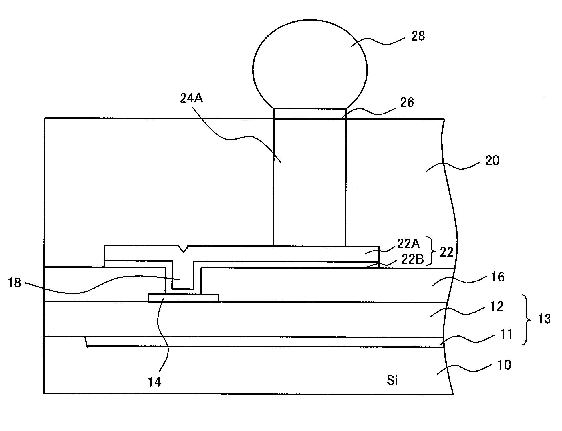
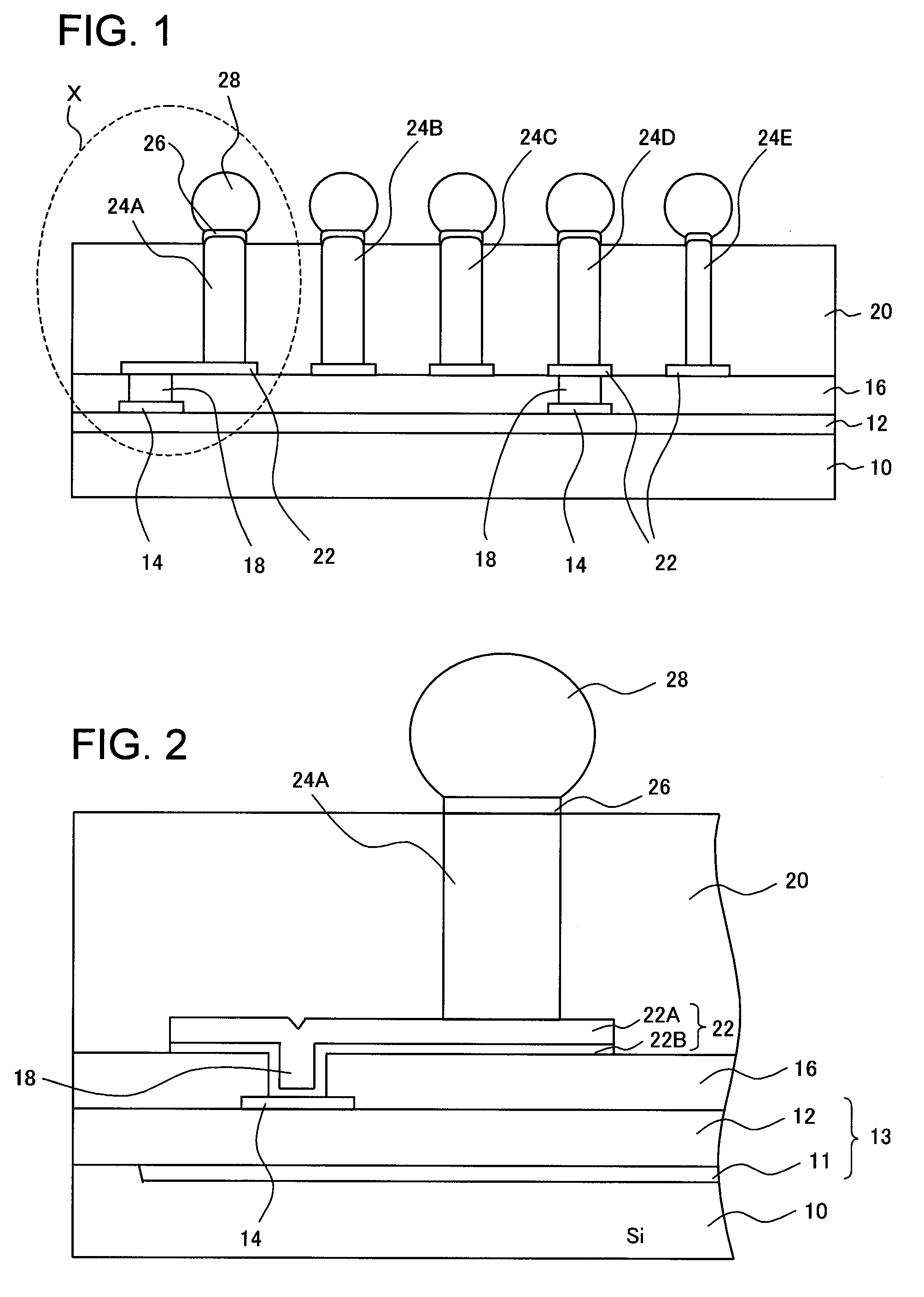
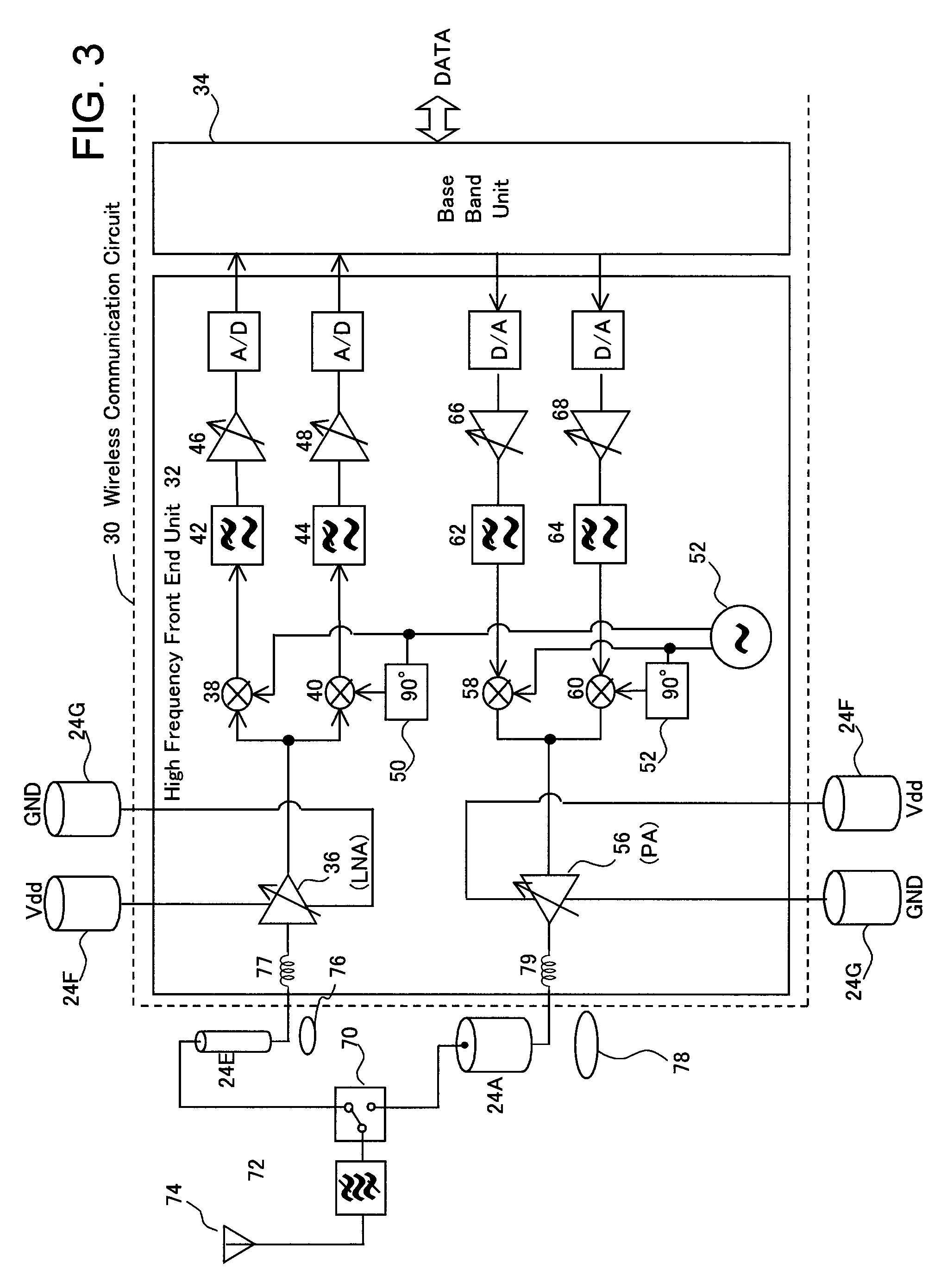
[0055]FIG. 1 is a cross-sectional view of a high-frequency device of the present embodiment. At the surface of a silicon semiconductor substrate 10, there are formed circuit elements such as transistors which together with a multilayer wiring layer 12 connecting the circuit elements constitutes a high-frequency circuit layer. The high-frequency circuit, as described hereinbelow, is composed of circuit elements such as transistors, an input, an output, a power source, ground, and the like. An electrically conductive pad 14 is formed as the topmost electrically conductive layer of the multilayer wiring layer 12 and connected to wiring (not shown in the figure) located inside the multilayer wiring layer 12. A first elec...


PUM


Abstract

A high-frequency device has a semiconductor substrate; a high-frequency circuit layer formed on the substrate and including a circuit element and a multilayer wiring layer; electrically conductive pads; rewiring layers connected to the electrically conductive pads; an electrically insulating sealing layer formed on the first electrically insulating layer and the rewiring layer and having a thickness larger than the multilayer wiring layer; electrically conductive posts provided inside the electrically insulating sealing layer and between the rewiring layer and the mounting connection terminals. A first electrically conductive post corresponding to a power source has a first diameter; a second electrically conductive post corresponding to an input of input amplifier has a second diameter less than the first diameter; and a third electrically conductive post corresponding to an output of power output amplifier has a third diameter larger than the second diameter.

Description

CROSS-REFERENCE TO RELATED APPLICATIONS [0001] This application is based upon and claims the benefit of priority from the prior Japanese Patent Application No. 2003-426204, filed on Dec. 24, 2003, the entire contents of which are incorporated herein by reference.BACKGROUND OF THE INVENTION [0002] 1. Field of the Invention [0003] The present invention relates to a high-frequency device in which a high-frequency circuit is integrated on a semi-conductor chip, more particularly to a high-frequency device whose size is decreased by using a chip sized package and high-frequency characteristic is improved. [0004] 2. Description of the Related Art [0005] Wide spread of portable communication apparatuses created a demand for low-cost, compact and highly functional devices which are to be mounted thereupon. There are high-frequency devices that use a silicon substrate in order to reduce cost. It was suggested to form high-frequency circuits on a silicon substrate rather than on more expensiv...

Claims


Application Information

Patent Timeline
Patent Type & Authority Applications(United States)
IPC IPC(8): H01L23/12H01L21/60H01L23/00H01L23/31H01L23/48H01L23/485H01L23/52H01L23/522
CPCH01L23/3114H01L23/5225H01L2924/13091H01L24/13H01L2224/1403H01L23/5227H01L24/10H01L2224/13099H01L2224/16H01L2924/01002H01L2924/01013H01L2924/01015H01L2924/01029H01L2924/01033H01L2924/01078H01L2924/01082H01L2924/10329H01L2924/14H01L2924/19041H01L2924/19042H01L2924/19043H01L2924/30105H01L2924/30107H01L2924/3011H01L2924/3025H01L2924/01005H01L2924/01006H01L2924/014H01L2924/00H01L24/02H01L24/05H01L24/06H01L24/14H01L2224/023H01L2224/05001H01L2224/05008H01L2224/05022H01L2224/05024H01L2224/05124H01L2224/05147H01L2224/05568H01L2224/05569H01L2224/056H01L2224/0603H01L2224/0616H01L2224/13H01L2924/0001H01L2924/00014H01L2224/02H01L23/12H01L21/60
Inventor KOBAYASHI, KAZUHIKOKONDO, FUMITAKA
Owner FUJITSU LTD
Learn More