Common voltage source integrated circuit for liquid crystal display device

a liquid crystal display device and integrated circuit technology, applied in pulse generators, instruments, pulse techniques, etc., can solve the problems of deteriorating image lowering the brightness of lcd devices, and failing to output the common voltage vcom properly, so as to improve the display quality of liquid crystal display devices

Active Publication Date: 2005-06-30
LG DISPLAY CO LTD
View PDF2 Cites 29 Cited by
  • Summary
  • Abstract
  • Description
  • Claims
  • Application Information

AI Technical Summary

Benefits of technology

[0014] An object of the present invention is to provide a common voltage source IC that prevents a signal delay of common voltage during common voltage sw...

Problems solved by technology

However, as shown in FIG. 4, the common voltage source IC of the related art does not output the common voltage Vcom properly in time when the data voltage is applied.
As a result, the image quali...

Method used


Image

  • Common voltage source integrated circuit for liquid crystal display device
  • Common voltage source integrated circuit for liquid crystal display device
  • Common voltage source integrated circuit for liquid crystal display device

Examples


first embodiment

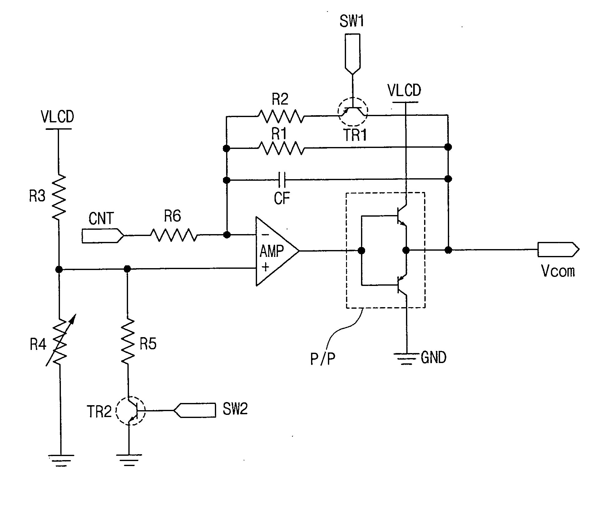
[0033]FIG. 5 is an exemplary circuit diagram of a common voltage source IC device according to the present invention. In FIG. 5, a common voltage source IC device may include an operational amplifier AMP and a push-pull circuit P / P. The operational amplifier AMP may be an inverting amplifier performing an inverting amplification and may include an inverting input (−), a non-inverting input (+), and an output. A control signal CNT may be applied to the inverting input (−) of the operational amplifier AMP via a sixth resistor (i.e., inverting resistor) R6. The control signal CNT may include a square waveform and may have a half pulse period of about 16.7 ms. The control signal CNT may induce common voltage swings, such that the common voltage Vcom may have a level change.

[0034] In addition, the push-pull circuit P / P may be connected to the operational amplifier output and a ground source GND. The push-pull circuit P / P also may receive a liquid crystal drive voltage VLCD and may output...

second embodiment

[0060] described hereinbefore, the first and second switching transistors TR1 and TR2 are P-type and N-type transistors, respectively, and then the combination resistors are induced by the first and second switching signals. However, other types of transistors or other structure of electric circuit may be possible for the common voltage source IC device. When the transistor type is changed, the switching signals will also be changed as shown in FIG. 9. Namely, if the first and second switching transistors TR1 and TR2 are N-type and P-type transistors, respectively, first and second signals shown in FIG. 9 are applied to the N-type first transistor TR1 and the P-type second transistor TR2, respectively.

[0061]FIG. 10 is an exemplary circuit diagram of a common voltage source IC device according to a third embodiment of the present invention. In FIG. 10, similar to the first and second embodiments, a common voltage source IC device may include an operational amplifier AMP and a push-p...

third embodiment

[0068] As described in FIG. 6, the first switching signal SW1 may change its state when the control signal CNT is rising, i.e., the control signal CNT is in transition from the low state to the high state. In addition, the second switching signal SW2 may change its state when the control signal CNT is falling, i.e., when the control signal CNT is in transition from the high state to the low state. In this third embodiment, it is assumed that the first and second switching transistors TR1 and TR2 (shown in FIG. 10) are all N-type transistors. Therefore, the first and second switching transistors TR1 and TR2 (shown in FIG. 10) may be turned ON when the first and second switching signals SW1 and SW2 are in the high state, and the first and second switching transistors TR1 and TR2 may be OFF when the first and second switching signals SW1 and SW2 (shown in FIG. 10) are in the low state.

[0069] With reference to FIGS. 6 and 10, when the first switching signal SW1 is in the low state, i.e....


PUM


Abstract

A common voltage source IC device includes an operational amplifier, a push-pull circuit receiving an output signal from the operational amplifier and outputting a common voltage to a common voltage terminal; an inverting resistor connected to an inverting input of the operational amplifier; a feedback resistor connected to the common voltage terminal and the inverting input; a capacitor connected to the common voltage terminal and the inverting input; a first switching resistor connected to the inverting input and a first switching transistor, the first switching transistor connected to the common voltage terminal; a driving resistor receiving a drive voltage and connected to a non-inverting input of the operational amplifier; a variable resistor connected to the non-inverting input and a ground source; and a second switching resistor connected to the non-inverting input and a second switching transistor, the second switching transistor connected to the ground source.

Description

[0001] The present invention claims the benefit of Korean Patent Application Nos. 2003-0100673 and 2004-0079839 filed on Dec. 30, 2003, and Oct. 7, 2004, respectively, which are hereby incorporated by reference. BACKGROUND OF THE INVENTION [0002] 1. Field of the Invention [0003] The present invention relates to liquid crystal display (LCD) devices, and more particular, to a common voltage source integrated circuit (IC) for an LCD device that reduces a common voltage delay and prevents a block dim and a waving noise in common voltage swings. [0004] 2. Discussion of the Related Art [0005] Until recently, display devices generally employed cathode-ray tubes (CRTs) or television monitors. Presently, many efforts are being made to study and develop various types of flat panel displays, such as liquid crystal display devices (LCDs), plasma display panel (PDPs), field emission displays, and electro-luminescence displays (ELDs), as substitutions for CRTs because of their high resolution ima...

Claims


Application Information

Patent Timeline
IPC IPC(8): G09G3/36H03B1/00
CPCG09G3/3655G09G3/3614
Inventor YI, SANG-YEOLKIM, KYONG-SEOK
Owner LG DISPLAY CO LTD
Why Eureka
Try Eureka