Exposure device, exposure method and device manufacturing method

a technology of exposure device and manufacturing method, which is applied in the direction of microlithography exposure apparatus, printers, instruments, etc., can solve the problems of deterioration in accuracy, deterioration in resolution, and variation in baseline amount (i.e., baseline drift) during exposure, so as to improve the performance of the exposure device and shorten the time wastage

Inactive Publication Date: 2005-06-30
NIKON CORP
View PDF4 Cites 31 Cited by
  • Summary
  • Abstract
  • Description
  • Claims
  • Application Information

AI Technical Summary

Benefits of technology

[0021] According to the present invention, because the second setting device and the control device are located away from the first setting device, and also closer to the vicinity of the object of control than the first setting device, it is possible to shorten time wastages due to control and, consequently, it is possible to set the temperature inside an exposure device to a target temperature with a high degree of accuracy, and the performance of the exposure device can be consistently maintained at the performance that is anticipated.
[0022] The device man...

Problems solved by technology

As a result, deterioration in the resolution and the like occurs and problems arise when a detailed pattern is being transferred.
Moreover, because thermal expansion and thermal deformation are generated in the alignment sensors and the stages by changes in temperature inside the exposure device, there is a concern that a variation in the baseline amount (i.e., baseline drift) will occur during exposure.
Because of this, the problem arises that a deterioration in accuracy occurs when the projected pattern and the shot area are overlayed.
In addition, the temperature of the atmosphere surrounding the stages is raised by the heat generated by the stages, and the problem arises that the stage positioning accuracy is worsened by the effects such as fluctuations in the optical path of the interferometer that measures the positions of the stages.
However, using as an example an exposure device that is provided with, for example, a liquid-cooled type of temperature control device, the diameter of pipes that are used to conduct temperature-controlled coolant in the vicinity of a Meat generating source such as a motor is restricted by the size of the exposure device and by space limitations inside the exposure device.
Moreover, because it is clearly not possible to use any optional component as a pipe, the pressure inside the pipes is restricted and the f...

Method used


Image

  • Exposure device, exposure method and device manufacturing method
  • Exposure device, exposure method and device manufacturing method
  • Exposure device, exposure method and device manufacturing method

Examples


first embodiment

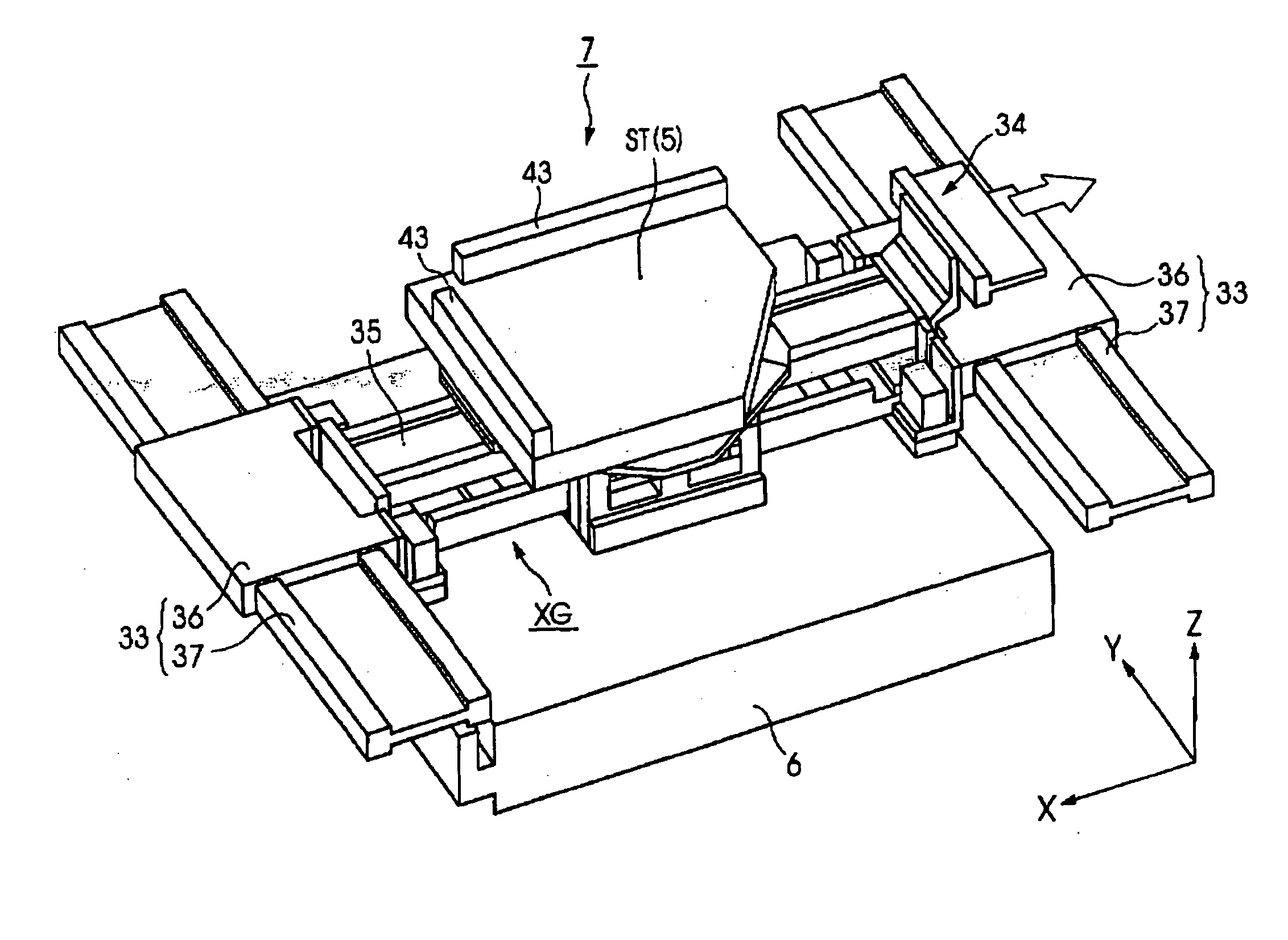
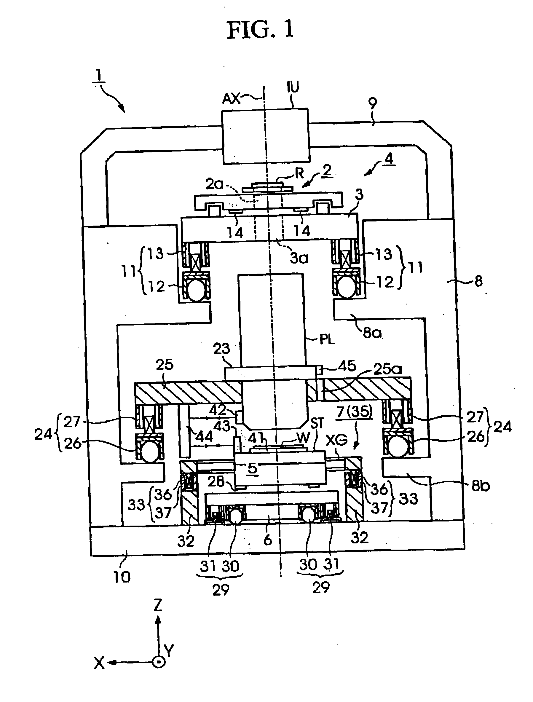
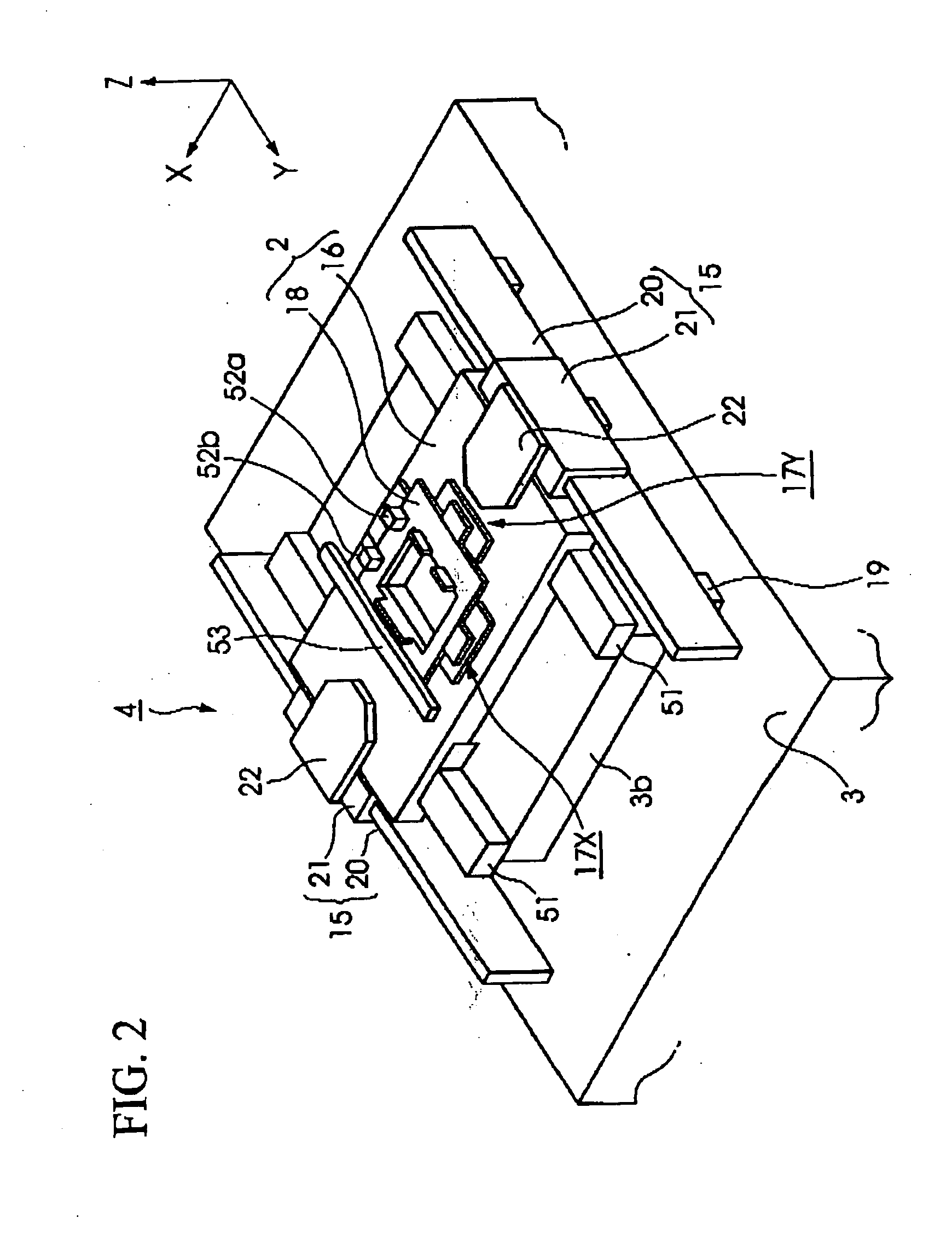
[0054]FIG. 1 is a schematic view of the entire exposure device according to the first embodiment of the present invention. In the present embodiment, a description is given using as an example a case in which the present invention is applied to a step-and-scan type exposure device that manufactures a semiconductor device by transferring a pattern that is formed on a reticle R onto a wafer W, while moving the reticle R serving as a mask and the wafer W serving as a substrate relatively to a projection optical system PL shown in FIG. 1.

[0055] In the description given below, the XYZ rectangular coordinate system shown in FIG. 1 is set, and a description is given of positional relationships between each member while referring to this XYZ rectangular coordinate system. In the XYZ rectangular coordinate system, the X axis and Y axis are set so as to be parallel to the wafer W, while the Z axis is set so as to be a perpendicular direction (i.e., in a direction along the optical axis AX of...

second embodiment

[0172]FIG. 13 is a schematic view of an exposure device according to the second embodiment of the present invention. In FIG. 13, the same symbols are allocated to members that correspond to members shown in the first embodiment, and a description thereof is omitted. As is shown in FIG. 13, the exposure device of the present embodiment can be broadly separated into an exposure chamber 140 that houses an exposure main body section 130 that is formed so as to include an illumination optical system IU, a reticle stage 2, a projection optical system PL, and a wafer stage 5 serving as subjects of control, and also a cooling apparats 143 that cools coolant circulating inside the exposure main body section 130.

[0173] The exposure chamber 140 that houses the exposure main body section 130 is placed on a floor F1 via seismic isolation pads 142 and 142. The cooling apparatus 143 is placed on a floor F2 that is positioned under the floor 1 via seismic isolation pads 144 and 144, so that the ex...

third embodiment

[0181] In the above described first embodiment and second embodiment, the temperature of the reticle stage 2 is determined by providing temperature sensors 76a and 76b that respectively detect the temperature of the coolant before it is circulated around the reticle stage 2 and the temperature of the coolant after it has circulated around the reticle stage 2, and then taking the average of these detection results. In addition, the temperature of the wafer stage 5 is determined by providing temperature sensors 79a and 79b that respectively detect the temperature of the coolant before it is circulated around the wafer stage 5 and the temperature of the coolant after it has circulated around the wafer stage 5, and then taking the average of these detection results.

[0182] However, as is shown in FIG. 14 and FIG. 15, it is also possible to directly detect the temperatures of the reticle stage 2 and the wafer stage 5. FIG. 14 is an external perspective view of a reticle stage that is pro...


PUM


Abstract

An exposure device, where circulating systems and for controlling a temperature varied by the driving of a linear motor are connected to a reticle stage and wafer stage, a controller sets the temperature of refrigerant circulating through the circulating system by driving heater, circulating system is connected to a projection optical system and a controller sets the temperature of refrigerant circulating through a circulating system by driving heater by a feedforward control to control the temperature of the refrigerant circulating through the circulating system.

Description

BACKGROUND OF THE INVENTION [0001] 1. Field of the Invention [0002] The present invention relates to an exposure device and exposure method which transfer a pattern formed on a mask or reticle onto a substrate such as a wafer, and also to a device manufacturing method for manufacturing semiconductor devices, liquid crystal display devices, image pickup devices, thin-film magnetic heads, and other devices using the exposure device and exposure method. [0003] 2. Description of Related Art [0004] In a photolithographic step, which is one of the steps for manufacturing semiconductor devices, liquid crystal display devices, image pickup devices, thin-film magnetic heads, and other devices, an exposure device is used that transfers a pattern that is formed on a mask or reticle (hereinafter, when referring to these generically, they will be referred to as masks) onto a wafer or glass or the like (hereinafter, when referring to these generically, they will be referred to as substrates) on w...

Claims


Application Information

Patent Timeline
IPC IPC(8): G03F7/20
CPCG03F7/70858G03F7/70891G03F7/70875
Inventor TSUJI, TOSHIHIKOKIMURA, TAKAAKINAGAHASHI, YOSHITOMO
Owner NIKON CORP
Why Eureka
Try Eureka