Semiconductor device with high dielectric constant insulator and its manufacture

a dielectric constant and semiconductor technology, applied in semiconductor devices, chemical vapor deposition coatings, coatings, etc., can solve the problems of increasing gate leak current and consumption power, increasing new problems, increasing leak current, etc., to reduce hysteresis and suppress the formation of trap levels in the film

Inactive Publication Date: 2005-06-30
FUJITSU MICROELECTRONICS LTD
View PDF20 Cites 23 Cited by
  • Summary
  • Abstract
  • Description
  • Claims
  • Application Information

AI Technical Summary

Benefits of technology

[0025] It is said that the flat band voltage changes with fixed charges and the hysteresis changes with trap levels. It can be considered that by suppressing the oxygen supply amount in film forming source gasses at the growth start and end stages, it is possible to suppress the formation of a reaction

Problems solved by technology

At such a thickness, tunnelling current starts flowing directly through the gate oxide film, resulting in an increase in gate leak current and consumption power.
As a new material having a high dielectric constant is adopted as the material of a gate insu

Method used


Image

  • Semiconductor device with high dielectric constant insulator and its manufacture
  • Semiconductor device with high dielectric constant insulator and its manufacture
  • Semiconductor device with high dielectric constant insulator and its manufacture

Examples


Embodiment Construction

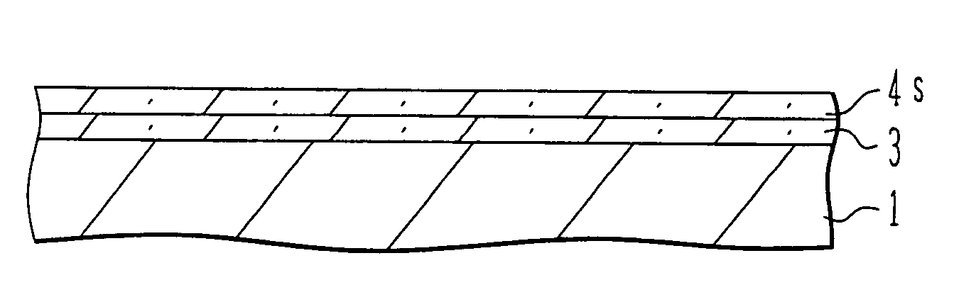
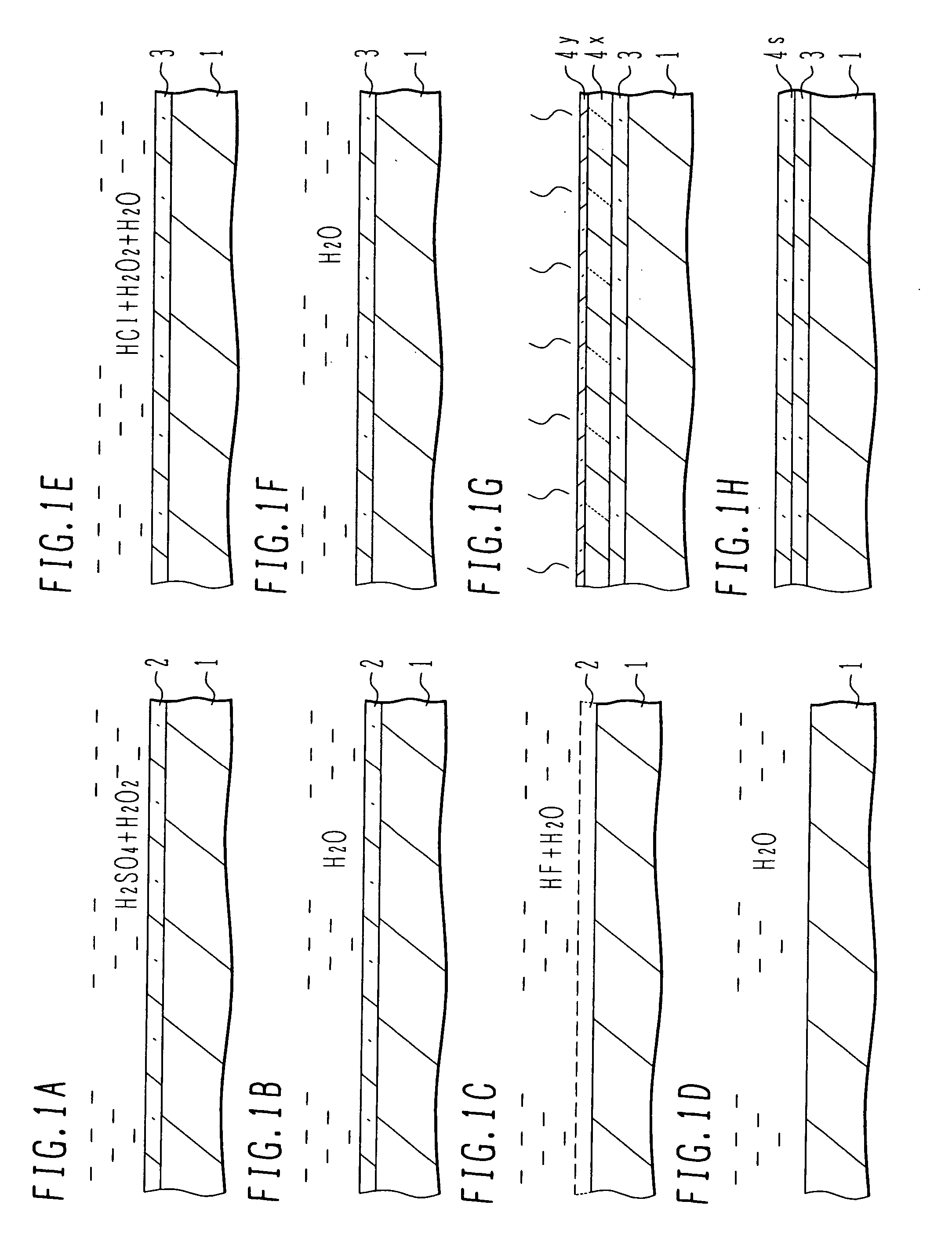
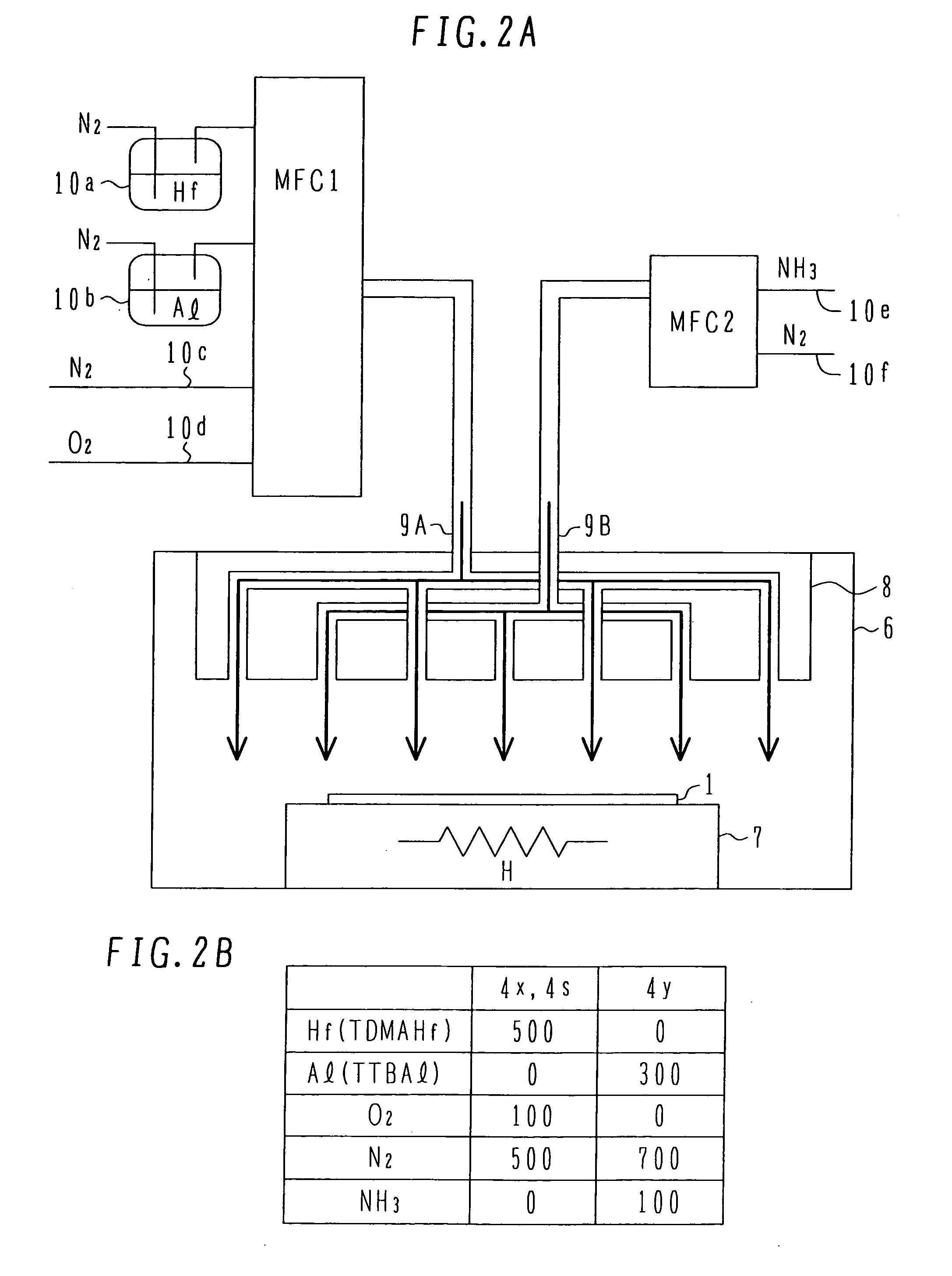
[0040] Hafnium oxide (hafnia) is insulator capable of providing a dielectric constant higher than silicon oxide by several to several tens times, and is highly expected as the gate insulating film of IG-FET. Thermal chemical vapor deposition (CVD) is known as a method capable of forming an oxide insulating film having a high dielectric constant such as hafnium oxide, with a good film quality and without adversely affecting the substrate.

[0041] As a silicon oxide layer is formed on the surface of a silicon substrate and a hafnium oxide film and a polysilicon film are formed on the silicon oxide film by thermal CVD to form an insulated gate structure, a flat band voltage shifts. It is therefore possible to control the threshold voltage. Since the oxide film between the hafnium oxide film and silicon substrate becomes thick, CET increases.

[0042] The present inventors presume that a reaction layer grows at the interface between a hafnium oxide film and a polysilicon layer and at other...


PUM

PropertyMeasurementUnit
Temperatureaaaaaaaaaa
Thicknessaaaaaaaaaa

Abstract

A semiconductor device has: a silicon substrate; a silicon oxide layer formed on the surface of the silicon substrate; a high dielectric constant insulating film including a first oxide layer formed above the silicon oxide layer and made of a high dielectric constant film having a dielectric constant higher than silicon oxide and a first nitride layer formed above the first oxide layer and made of nitride having an oxygen intercepting capability, or a high dielectric constant insulating film including a first oxide film formed on the silicon oxide layer, a second oxide layer formed on the first oxide layer and a third oxide layer formed on the second oxide layer, the first and third oxide layers having an oxygen diffusion coefficient smaller than the second oxide layer; and a gate electrode formed on the high dielectric constant insulating layer and made of oxidizable material.

Description

CROSS REFERENCE TO RELATED APPLICATION [0001] This application is based on and claims priorities of Japanese Patent Applications No. 2003-432555 filed on Dec. 26, 2003, No. 2003-431910 filed on Dec. 26, 2003 and No. 2004-238211 filed on Aug. 18, 2004, the entire contents of which are incorporated herein by reference. BACKGROUND OF THE INVENTION [0002] A) Field of the Invention [0003] The present invention relates to a semiconductor device and its manufacture method, and more particularly to a semiconductor device having a high dielectric constant oxide insulating film and its manufacture method. [0004] B) Description of the Related Art [0005] As representative semiconductor elements used in a semiconductor integrated circuit device, insulated gate (IG) type field effect transistors (FET) typically MOS transistors are widely used. For high integration of semiconductor integrated circuit devices, IG-FETs have been miniaturized based upon the scaling rules. Miniaturization reduces the ...

Claims


Application Information

Patent Timeline
IPC IPC(8): C23C16/40H01L21/28H01L21/314H01L21/316H01L21/8242H01L29/51H01L29/78
CPCC23C16/40C23C16/405H01L21/28167H01L21/28194H01L21/28202H01L29/7833H01L21/31645H01L29/513H01L29/517H01L29/518H01L21/3143H01L21/02164H01L21/02172H01L21/022H01L21/0217
Inventor SAKODA, TSUNEHISASUGIYAMA, YOSHIHIROYAMAGUCHI, MASAOMIMINAKATA, HIROSHI
Owner FUJITSU MICROELECTRONICS LTD
Why Eureka
Try Eureka