Method of forming bump pad of flip chip and structure thereof

a technology of flip chips and bump pads, which is applied in the direction of electrical equipment, semiconductor devices, semiconductor/solid-state device details, etc., can solve the problems of affecting the size and performance of the chip, the above bump forming process is difficult to perform, and the space between neighboring pads cannot be reached. , to achieve the effect of excellent electrical characteristics, high reliability and fine circuits

Inactive Publication Date: 2005-06-30
SAMSUNG ELECTRO MECHANICS CO LTD
View PDF5 Cites 8 Cited by
  • Summary
  • Abstract
  • Description
  • Claims
  • Application Information

AI Technical Summary

Benefits of technology

[0043] Therefore, it is an object of the present invention to alleviate the problems encountered in the related art and to provide a method of forming a bump pad of a flip chip, which is advantageous in terms of fine circuits, excellent electrical characteristics, high reliability, high-speed signal transfer structure, and high functionality.

Problems solved by technology

Particularly, it is known that the packaging and inspection steps constitute 70% of total fabrication costs, in which the packaging step greatly affects the size and performance of the chip.
However, the above bump forming process is difficult to perform, because the bumps each are selectively formed at a desired height on every fine pad.
However, the above method is disadvantageous in that the resulting flip chip pad is trapezoid in shape and has a bottom surface area which is larger than an allowed size, and thus, it is impossible to attain sufficient spaces between the neighboring pads.
However, the electrolytic copper pulse plating process suffers from largely deposited crystal structure.
Thus, an intercrystalline etching process by an acid of a post process results in a very uneven surface.
Hence, bonding on the flip chip is difficult due to the uneven surface or solder resist remainder with respect to the uneven surface.

Method used


Image

  • Method of forming bump pad of flip chip and structure thereof
  • Method of forming bump pad of flip chip and structure thereof
  • Method of forming bump pad of flip chip and structure thereof

Examples


Embodiment Construction

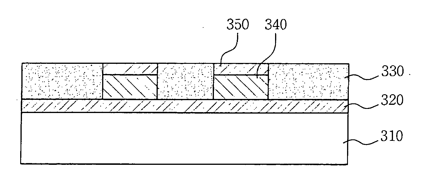
[0055] Hereinafter, a detailed description will be given of a method of forming a bump pad of a flip chip of the present invention, with reference to the appended drawings.

[0056]FIGS. 3a through 3f are sectional views sequentially showing the fabrication of the bump pad, according to the present invention.

[0057] As shown in FIG. 3a, an insulating layer 310 is plated via an electroless copper plating process, whereby a thin copper plating layer 320 is formed thereon, which can be electrically conducted.

[0058] The electroless plating or metal sputtering or metal sputtering or metal sputtering process is solely used to provide electroconductivity to the surface of the insulating material, such as resins, ceramics and glass.

[0059] Hence, the electroless copper plating is performed not by ionic reactions but by deposition reactions, in which the deposition is accelerated by a catalyst.

[0060] With the aim of depositing copper from a plating solution, the catalyst should be attached o...


PUM


Abstract

Disclosed is a method of forming a bump pad of a flip chip and a structure thereof, characterized in that a resist pattern is formed through coating of a photosensitive material on an electroless copper plating layer, exposure to light and development, and then a bump pad is prepared by pulse plating and direct current plating of the resist pattern, thereby fabricating a substrate with a high density and high reliability.

Description

BACKGROUND OF THE INVENTION [0001] 1. Field of the Invention [0002] The present invention relates, in general, to formation methods of bump pads of flip chips and structures thereof. More particularly, the present invention relates to a method of fabricating a bump pad of a flip chip, characterized in that a photosensitive material is coated on an electroless copper plating layer, exposed to light and developed, to prepare a resist pattern, which is then subjected to pulse plating and direct current plating, to form a bump pad, thereby obtaining a substrate with a high density and high reliability; and a structure of the bump pad of the flip chip. [0003] 2. Description of the Related Art [0004] In general, a fabrication method of a semiconductor comprises three steps of manufacturing, packaging, and inspection of a silicon chip. Particularly, it is known that the packaging and inspection steps constitute 70% of total fabrication costs, in which the packaging step greatly affects the...

Claims


Application Information

Patent Timeline
Patent Type & Authority Applications(United States)
IPC IPC(8): H01L21/28H01L21/44H01L21/48H01L21/50H01L21/60H01L23/48H01L23/485
CPCH01L24/10H01L24/11H01L24/13H01L2924/10253H01L2924/014H01L2224/13099H01L2924/01011H01L2924/01013H01L2924/01022H01L2924/01029H01L2924/0103H01L2924/01033H01L2924/01046H01L2924/01078H01L2924/01079H01L2924/01082H01L2924/01322H01L2924/09701H01L2924/01005H01L2924/01006H01L2924/01019H01L2924/01024H01L2924/00H01L2924/351H01L2924/15787H01L2224/1134H01L2224/13144H01L2224/13H01L2924/00014H01L21/60
Inventor HAZE, TAKAYUKI
Owner SAMSUNG ELECTRO MECHANICS CO LTD
Why Eureka
Try Eureka