Method for reduced N+ diffusion in strained Si on SiGe substrate

a technology of strained sige and substrate, which is applied in the direction of semiconductor devices, electrical devices, transistors, etc., can solve the problems of increasing the diffusion of implanted n-type impurities, difficult to achieve consistent roll-off device characteristics, and n-type impurities are easily implanted, so as to reduce the diffusion of n-type impurities and reduce the vacancy concentration

Inactive Publication Date: 2005-07-07
GLOBALFOUNDRIES INC
View PDF99 Cites 1 Cited by
  • Summary
  • Abstract
  • Description
  • Claims
  • Application Information

AI Technical Summary

Benefits of technology

[0005] In an aspect of the invention, a method for manufacturing a semiconductor device Is provided. The method includes the step of forming the source and drain extension regions in an upper surface of a SiGe-based substrate. The source and drain extension regions contain an N type impurity. Then, vacancy concentration in the source and drain extension regions is reduced in order to reduce diffusion of the N type impurity contained in the source and drain extension regions. The vacancy concentration is reduced by providing an interstitial element or a vacancy-trapping element in the source and drain extension.
[0006] In another aspect of the invention, a method is provided for reducing diffusion of an N type impurity in a SiGe-based substrate. Source and drain extension regions are in an upper surface of the SiGe-based substrate. An interstitial element or a vacancy-trapping element is Ion-implanted into the source and drain extension regions to reduce vacancy concentration in the source and drain extension regions.

Problems solved by technology

The SiGe-based substrate, however, exhibits certain drawbacks, especially when NFET devices are formed thereon.
Here, the excessive amount of vacancies contained in the SiGe layer undesirably increases diffusion of the implanted N type impurity.
This makes it more difficult to achieve consistent roll-off device characteristics.

Method used


Image

  • Method for reduced N+ diffusion in strained Si on SiGe substrate
  • Method for reduced N+ diffusion in strained Si on SiGe substrate
  • Method for reduced N+ diffusion in strained Si on SiGe substrate

Examples


Embodiment Construction

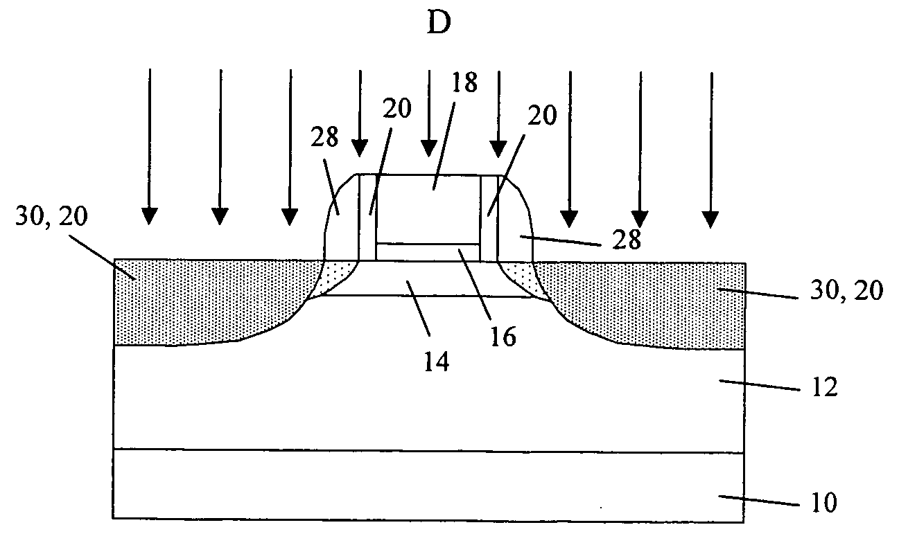
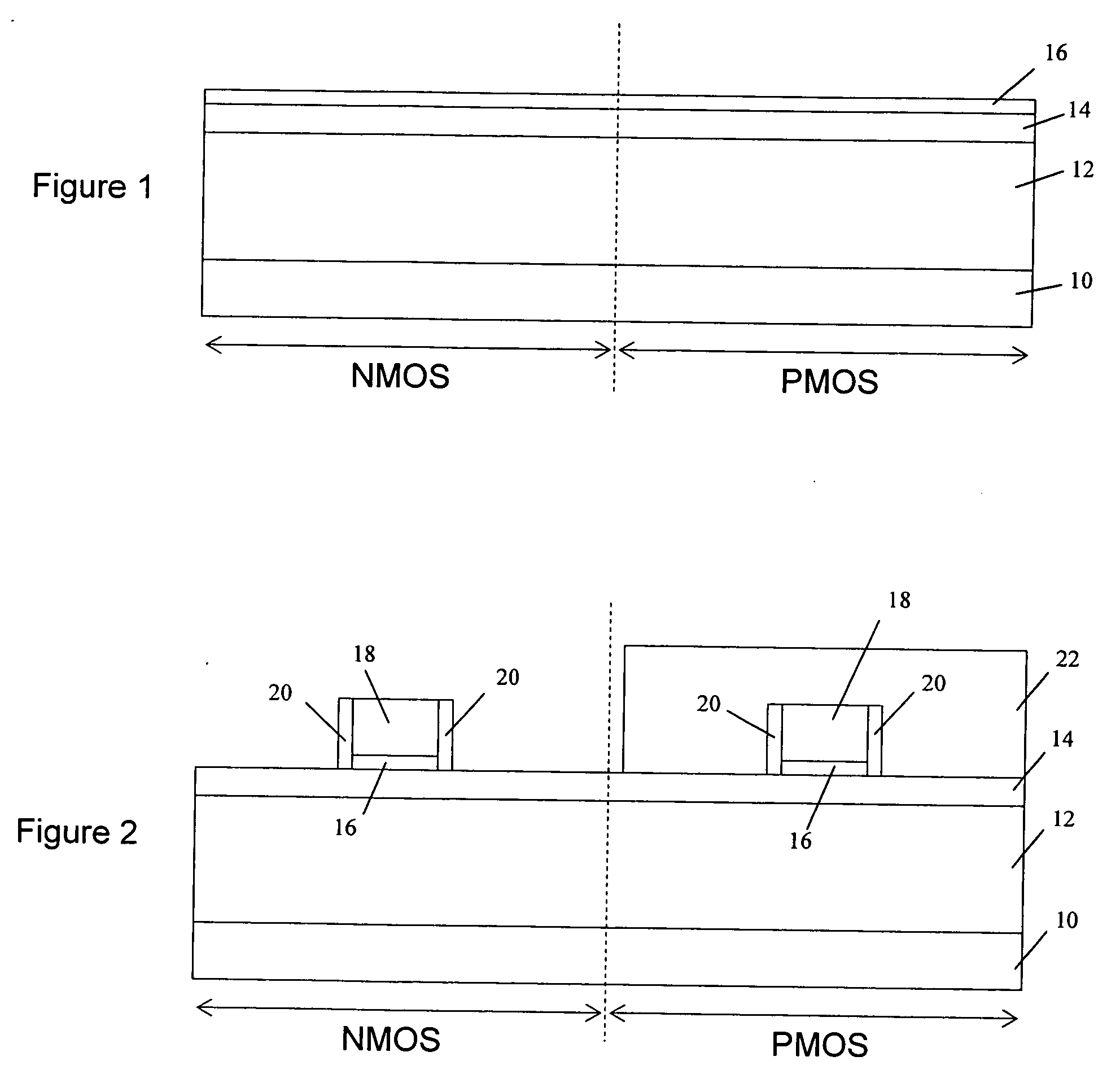
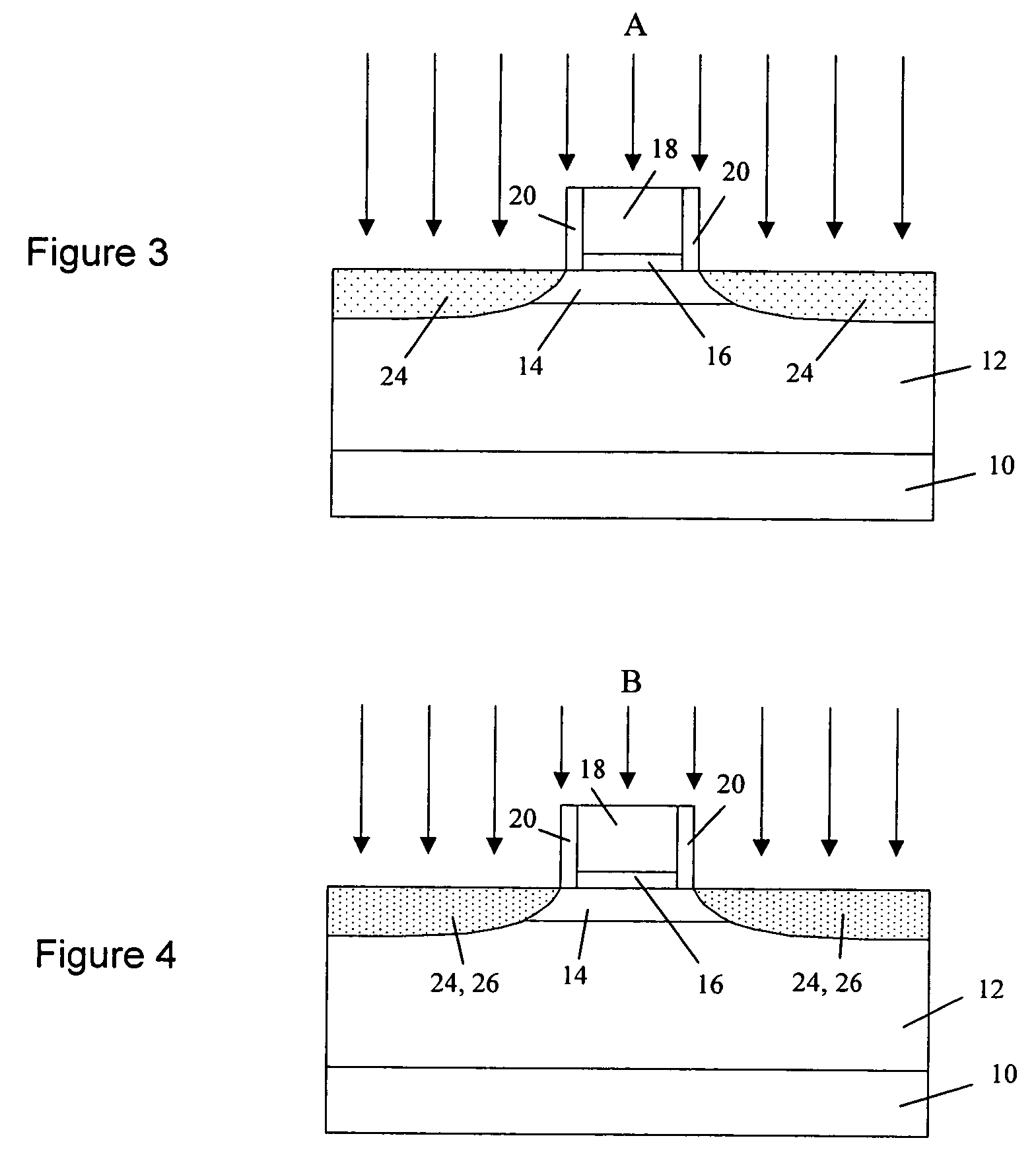
[0010] The invention provides a method that significantly reduces undesirable diffusion of the N type impurity in a SiGe-based substrate, thereby improving roll-off characteristics of devices. In an embodiment, the diffusion of N type impurity Is reduced by reducing vacancies in source and drain extension regions. The vacancies are reduced by providing an interstitial element (e.g., Si or O) or a vacancy-trapping element (e.g., F, N, Xe, Ar, He, Kr or a noble gas element) to the source and drain extension regions.

[0011] Typically, the interstitial element creates an additional interstitial per every ion provided thereto, and the additional interstitials react with and annihilate excessive vacancies in the SiGe-based substrate. The vacancy-trapping element trap vacancies and form vacancy-based clusters. Since vacancies are either annihilated or trapped by the interstitial element or the vacancy-trapping element, vacancy concentration Is reduced, thereby reducing diffusion of the N t...


PUM


Abstract

The first source and drain regions are formed in an upper surface of a SiGe substrate. The first source and drain regions containing an N type impurity. Vacancy concentration in the first source and drain regions are reduced in order to reduce diffusion of the N type impurity contained In the first source and drain regions. The vacancy concentration Is reduced by an interstitial element or a vacancy-trapping element in the first source and drain regions. The interstitial element or the vacancy-trapping element is provided by ion-implantation.

Description

BACKGROUND OF INVENTION [0001] The invention relates to methods for manufacturing a semiconductor device with improved device performance and a device structure exhibiting the improved device performance, and more particularly to a method for manufacturing a SiGe-based device exhibiting reduced diffusion of an N type impurity. [0002] The escalating requirements for ultra large scale integration semiconductor devices require ever increasing high performance and density of transistors. With scaling-down of a device dimension reaching limits, the trend has been to seek new materials and methods that enhance device performance. One of the most preferred methods is through mobility enhancement. [0003] It is known that biaxial tensile strain applied to a channel region increases electron mobility in NFET devices. This can be achieved by building an NFET device, which is composed of a set of stacked films (e.g., silicon-SiGe-silicon) on a substrate. Starting from a silicon substrate, SiGe ...

Claims


Application Information

Patent Timeline
Patent Type & Authority Applications(United States)
IPC IPC(8): H01L21/265H01L21/332H01L21/336H01L21/461H01L21/8234H01L21/8238H01L29/10H01L29/78H01L31/117
CPCH01L21/26506H01L21/26513H01L29/6656H01L29/1054H01L21/823814H01L21/26566
Inventor CHIDAMBARRAO, DURESETIDOKUMACI, OMER H.
Owner GLOBALFOUNDRIES INC
Why Eureka
Try Eureka