Polishing pad, platen hole cover, polishing apparatus, polishing method, and method for fabricating semiconductor device

a technology of platen hole cover and polishing pad, which is applied in the direction of edge grinding machine, flexible wheel, manufacturing tools, etc., can solve the problems of inability to achieve satisfactory measurement accuracy, scattered light reflected at and easy scratching on the surface of the substra

Inactive Publication Date: 2005-07-07
TORAY IND INC
View PDF0 Cites 59 Cited by
  • Summary
  • Abstract
  • Description
  • Claims
  • Application Information

AI Technical Summary

Benefits of technology

[0024] In accordance with the present invention, it is possible to provide a windowed polishing pad or a platen hole cover which is used to form planar surfaces in glass, semiconductors, dielectric / metal composites, integrated circuits, etc.; a polishing apparatus including the windowed polishing pad or the platen hole cover; a method for fabricating a semiconductor device using the polishing apparatus; and a polishing method, in which the number of scratches occurring on the surface of the substrate is small, and the polished state can be optically measured satisfactorily through the windowed polishing pad or the platen hole cover during polishing.

Problems solved by technology

However, in the polishing pad using such a transparent solid uniform resin for the window member, since the window member comes into contact with the surface of the substrate, i.e., the surface to be polished, scratches easily occur on the surface of the substrate, which is problematic.
Moreover, since the window member does not uniformly come into contact with the surface of the substrate, i.e., the surface to be polished, the slurry is interposed between the window member and the surface of the substrate.
As a result, light reflected at the surface of the substrate is scattered, and it is not possible to achieve satisfactory measurement accuracy, which is also problematic.

Method used


Image

  • Polishing pad, platen hole cover, polishing apparatus, polishing method, and method for fabricating semiconductor device
  • Polishing pad, platen hole cover, polishing apparatus, polishing method, and method for fabricating semiconductor device
  • Polishing pad, platen hole cover, polishing apparatus, polishing method, and method for fabricating semiconductor device

Examples


example 1

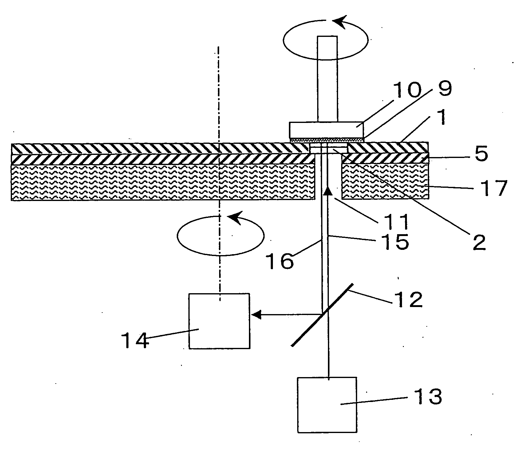
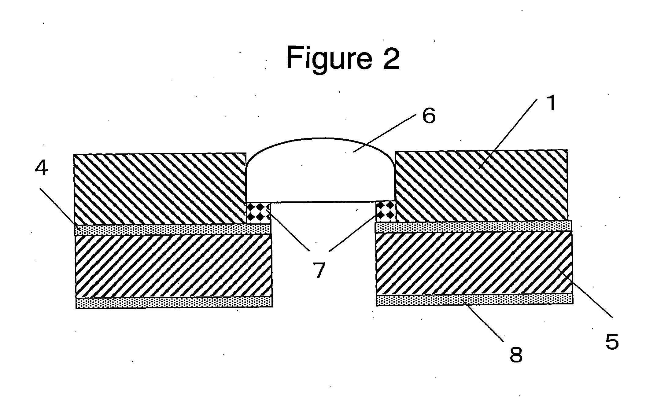
[0138] A transparent window member composed of transparent ABS was prepared by molding Toyolac 920 (transparent ABS resin) manufactured by Toray Industries, Inc. at a molding temperature of 60 to 80° C. The transparent window member had a thickness of 0.4 mm, a width of 18.5 mm, and a length of 56.5 mm. In the transparent window member, four corners and four edges of the upper surface were rounded with a radius of 0.4 mm. The micro rubber A-type hardness of the light-transmissive window member was 99 degrees. A polishing pad was fabricated by bonding an NBR rubber sheet with a thickness of 1 mm to a Rodel IC-1000. An opening of 19.5×57.5 mm was formed in the polishing pad at the position corresponding to the platen hole. A double-sided tape 442J manufactured by Sumitomo 3M Ltd. was attached to the rubber sheet side of the polishing pad having the opening, and a cutout of 13×50 mm was formed in the double-sided tape in the center of the opening. A highly deformable member composed of...

example 2

[0139] A transparent window member composed of transparent ABS was prepared as in Example 1. A highly deformable member composed of EPT sponge EPT#300 manufactured by Daiwabo Co., Ltd. with a thickness of 1.7 mm was prepared. Double-sided tapes 442J manufactured by Sumitomo 3M Ltd. were attached to both surfaces of the highly deformable member with a size of 18.5×56.5 mm, and a cutout of 13×50 mm was formed in the center. The transparent window member and the cushioning member were laminated on each other to form a platen hole cover. A polishing pad was fabricated by bonding an NBR rubber sheet with a thickness of 1 mm to a Rodel IC-1000 and attaching a double-sided tape 442J manufactured by Sumitomo 3M Ltd. to the back surface of the rubber. An opening of 21×59 mm was formed in the polishing pad at the position corresponding to the platen hole. When a weight of 3,000 g was applied to the light-transmissive window member of the platen hole cover with a pressing jig having a contact ...

example 3

[0141] By polymerization of MMA, a PMMA sheet with a thickness of 0.3 mm was formed, and the PMMA sheet was coated with one-part silicone SE9185 manufactured by Toray-Dow Corning Silicone Co., Ltd. at a thickness of 0.3 mm. Thereby, a transparent window member with a thickness of 0.6 mm and a size of 18.5 a 56.5 mm was fabricated. The silicone rubber layer had a micro rubber A-type hardness of 50 degrees, and the PMMA layer had a micro rubber A-type hardness of 99 degrees. A polishing pad was fabricated by bonding a foamed polyurethane sheet with a thickness of 1 mm and a density of 0.1 to a Rodel IC-1000. An opening of 19.5×57.5 mm was formed in the polishing pad at the position corresponding to the platen hole. A double-sided tape 442J manufactured by Sumitomo 3M Ltd. was attached to the foamed polyurethane side of the polishing pad having the opening, and a cutout of 13×50 mm was formed in the double-sided tape in the center of the opening. A highly deformable member composed of ...


PUM


Abstract

It is an object of the present invention to provide a windowed polishing pad or a platen hole cover which is used to form planar surfaces in glass, semiconductors, dielectric/metal composites, integrated circuits, etc.; a polishing apparatus including the windowed polishing pad or the platen hole cover; a method for fabricating a semiconductor device using the polishing apparatus; and a polishing method, in which the number of scratches occurring on the surface of the substrate is small, and the polished state can be optically measured satisfactorily during polishing. In order to achieve the above object, a polishing pad is constructed in such a manner that the polishing pad includes a polishing layer and a light-transmissive window member disposed in an opening formed in a part of the polishing layer, wherein the amount of indentation strain measured when a constant load is applied to substantially the entire upper surface of the light-transmissive window member is larger than the amount of indentation strain measured when the same constant load is applied to a region having the same area on the upper surface of the polishing layer.

Description

TECHNICAL FIELD [0001] The present invention relates to a windowed polishing pad which is suitable for use to form planar surfaces in semiconductors, dielectric / metal composites, integrated circuits, etc.; a platen hole cover; a polishing apparatus including the windowed polishing pad or the platen hole cover; and a method for fabricating a semiconductor device using the polishing apparatus. BACKGROUND ART [0002] As the density of semiconductor devices is increasing, multilevel interconnections and techniques associated therewith, for example, techniques for forming interlayer insulating films and techniques for forming electrodes using plug processes, damascene processes, or the like are becoming important. Accordingly, planarization processes for such interlayer insulating films and metal films of electrodes are also becoming important. As an efficient technique for the planarization processes, a polishing technique referred to as chemical mechanical polishing (CMP) is widely used...

Claims


Application Information

Patent Timeline
Patent Type & Authority Applications(United States)
IPC IPC(8): B24B37/20B24D13/14
CPCB24B37/205H01L21/304
Inventor SHIRO, KUNIYASUKOBAYASHI, TSUTOMUHASHISAKA, KAZUHIKO
Owner TORAY IND INC
Why Eureka
Try Eureka