

Semiconductor device
a technology of semiconductors and devices, applied in the direction of semiconductor devices, basic electric elements, electrical equipment, etc., can solve the problems of increased breakdown potential, increased loss in a mounted state for use, increased cost, etc., and achieves the effect of reducing the length of impurity diffusion, facilitating inversion of channel surfaces, and facilitating leakage current occurren
- Summary
- Abstract
- Description
- Claims
- Application Information
AI Technical Summary
Benefits of technology
Problems solved by technology
Method used
Image

Examples
first embodiment
[0054]FIG. 5 is a schematic plan view of a semiconductor device (semiconductor chip) with a vertical insulated gate field effect transistor (vertical high breakdown voltage MOSFET) built therein according to an embodiment (first embodiment) of the present invention. As shown in FIG. 5, a semiconductor device 1 is of a flat structure having, for example, a length of 4.0 mm, a width of 4.0 mm and a thickness of 0.4 mm. The whole of an upper surface of the semiconductor device 1 serves as a MOS unit cell area 2, in which there are formed a gate pad (gate bonding area) 3 as an external electrode terminal and a source pad (source bonding area) 4. A field limiting area spreads outside the MOS unit cell area 2. A back side of the semiconductor device 1 serves as a drain electrode.
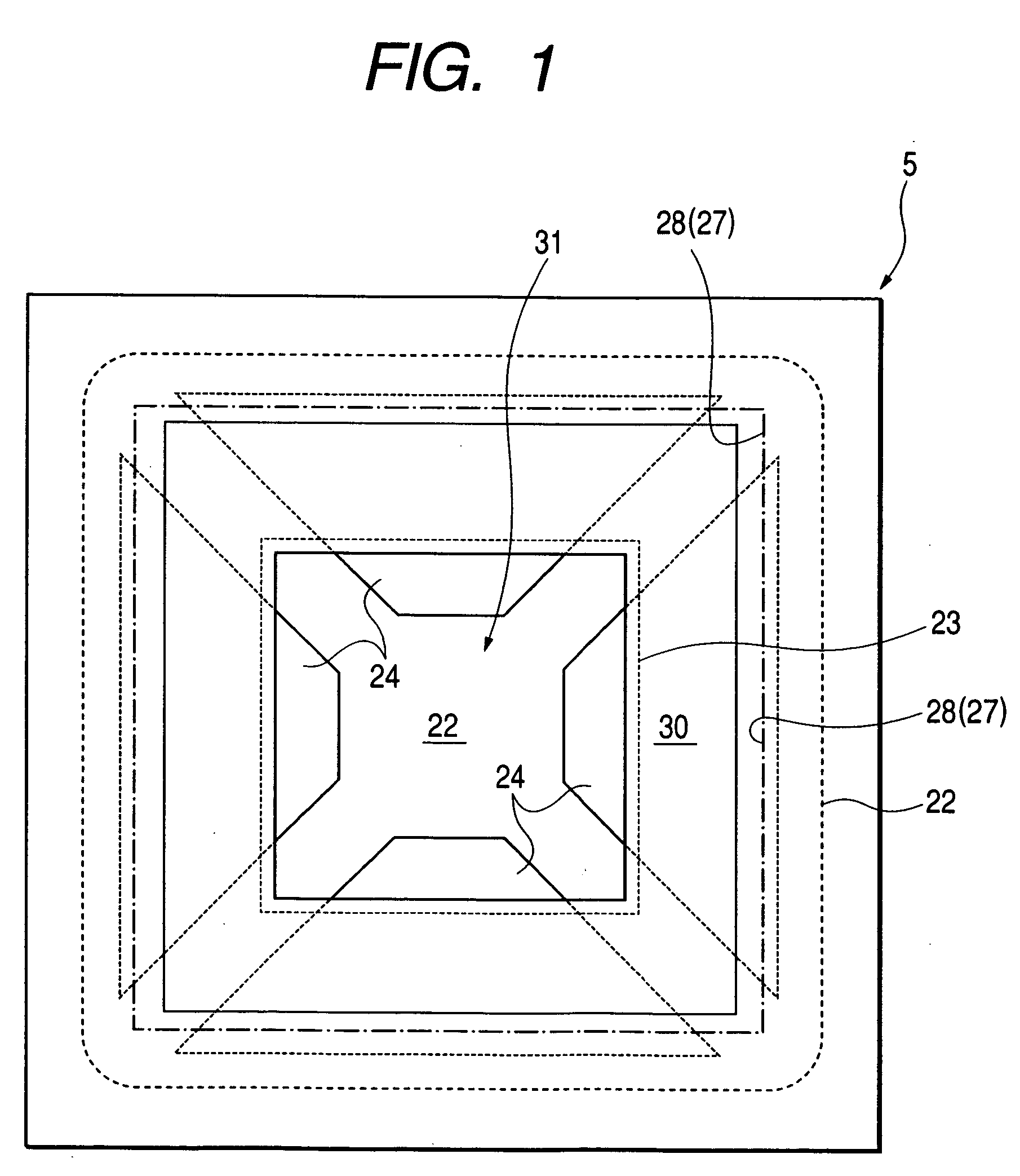
[0055]FIG. 6 is a schematic plan view showing the MOS unit cell area 2 partially. As shown in the same figure, unit MOSFETs (cells) 5 are arranged in order longitudinally and transversely. In the present inventio...
second embodiment
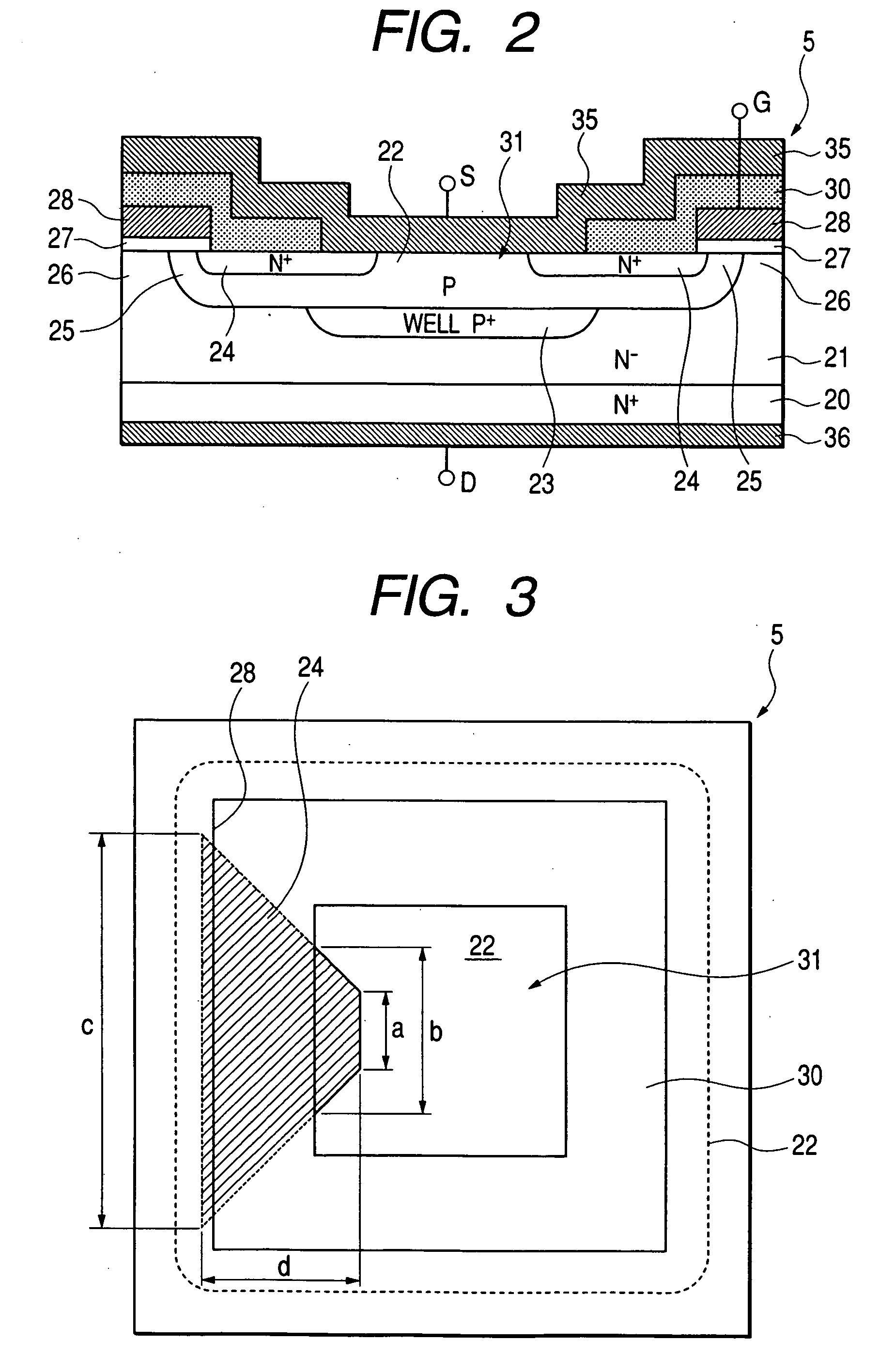
[0091]FIG. 9 is a schematic plan view showing a vertical power MOSFET portion according to a further embodiment (second embodiment) of the present invention and FIGS. 10(a) and 10(b) are sectional views taken along lines A-A′ and B-B′ in FIG. 9.
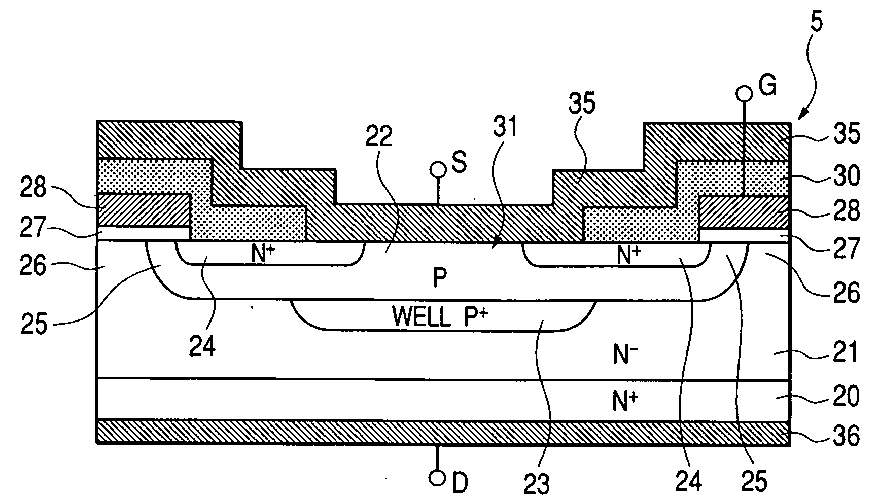
[0092] In this second embodiment, in a unit MOSFET (cell) 5, a source region 24 is formed as a quadrangular frame pattern extending along a source contact hole 31, but at the corners of a quadrangular cell the impurity concentration is not uniform and the channel length is short, so at the corner portions the source region 24 is not provided. FIG. 10(b) is a sectional view taken along line B-B′ in FIG. 9. In the same figure, the source region 24 extends up to below a gate insulating film 27 and a gate electrode 28 and a channel 25 is formed. FIG. 10(a) is a sectional view taken along line A-A′ in FIG. 9, showing a portion corresponding to a corner of a quadrangular cell. As shown in the same figure, an outer end portion of the source region ...
PUM
 Abstract
Description
Claims
Application Information