Field emission backlight unit, method of driving the backlight unit, and method of manufacturing lower panel

a backlight unit and field emission technology, applied in the field of backlight units for liquid crystal displays, can solve the problems of high manufacturing cost, high power consumption when light is reflected and transmitted, image cannot be viewed in a dark place, etc., and achieve the effect of uniform brightness and prolonging li

Inactive Publication Date: 2005-07-14
SAMSUNG SDI CO LTD
View PDF4 Cites 37 Cited by
  • Summary
  • Abstract
  • Description
  • Claims
  • Application Information

AI Technical Summary

Benefits of technology

[0011] The present invention provides a field emission backlight unit having a triod...

Problems solved by technology

Among these flat panel displays, LCDs have the advantages of light weight and low power consumption, but have a disadvantage in that, since they form an image not by emitting light by itself but by receiving light from an outside source, the image cannot be viewed in a dark place.
However, the conventional backlight unit is disadvantageous in that, since its structure is complex, manufacturing costs are high, and since the light source is disposed at the side of the backlight unit, power consumption is high when light is reflected and transmitted.
In ...

Method used


Image

  • Field emission backlight unit, method of driving the backlight unit, and method of manufacturing lower panel
  • Field emission backlight unit, method of driving the backlight unit, and method of manufacturing lower panel
  • Field emission backlight unit, method of driving the backlight unit, and method of manufacturing lower panel

Examples


Embodiment Construction

[0038] The present invention will now be described more fully with reference to the accompanying drawings, in which preferred embodiments of the invention are shown. In the drawings, whenever the same element reappears in a subsequent drawing, it is denoted by the same reference numeral.

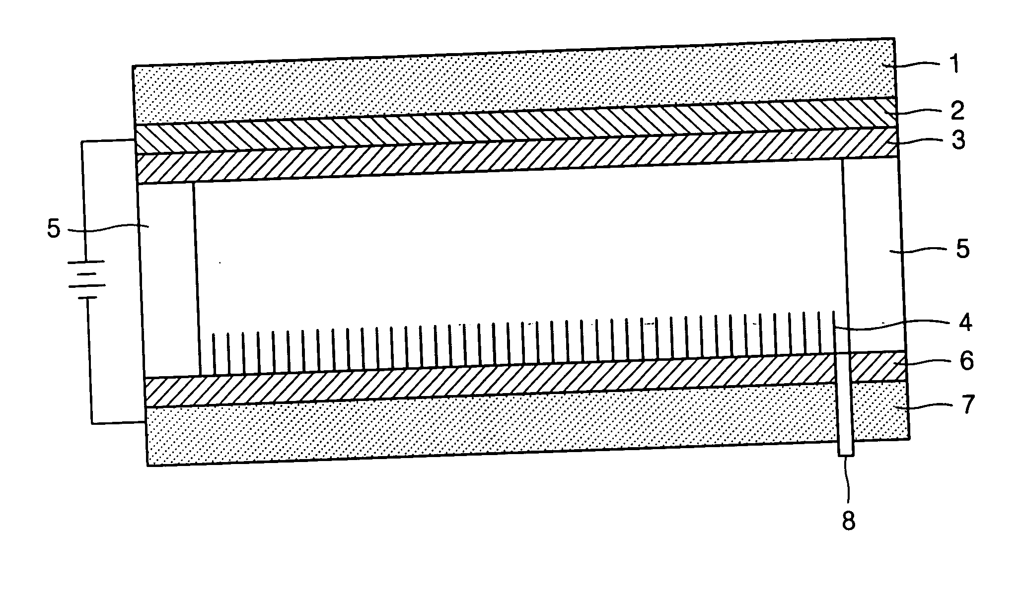
[0039]FIG. 1 is a cross-sectional view of a field emission backlight unit. Referring to FIG. 1, an indium tin oxide (ITO) electrode layer 2 and a fluorescent layer 3 are sequentially stacked on a bottom surface of an upper substrate 1. A thin metal layer 6 and a carbon nanotube layer 4 are sequentially stacked on a lower substrate 7. The upper substrate 1 and the lower substrate 7 are bonded to each other with a spacer 5 therebetween. A glass tube 8 for vacuum ventilation is installed in the lower substrate 7.

[0040] In the backlight unit constructed as above, if a voltage is applied between the ITO electrode layer 2 and the thin metal layer 6, electrons are emitted from the carbon nanotube layer 4 ...


PUM


Abstract

A field emission backlight unit for a liquid crystal display (LCD) includes: a lower substrate; first electrodes and second electrodes alternately formed in parallel lines on the lower substrate; emitters disposed on at least the first electrodes; an upper substrate spaced apart from the lower substrate by a predetermined distance such that the upper and lower substrates face each other; a third electrode formed on a bottom surface of the upper substrate; and a fluorescent layer formed on the third electrode. Since the backlight unit has a triode-type field emission structure, field emission is very stable. Since the first electrodes and the second electrodes are formed in the same plane, brightness uniformity is improved and manufacturing processes are simplified. If the emitters are disposed on both the first electrodes and the second electrodes, and a cathode voltage and a gate voltage are alternately applied to the first electrodes and second electrodes, the lifespan and brightness of the emitters can be improved. The above advantages are also achieved as a result of the method of driving the backlight unit and the method of manufacturing the lower panel thereof.

Description

CLAIM OF PRIORITY [0001] This application makes reference to, incorporates the same herein, and claims all benefits accruing under 35 U.S.C. §119 from an application for FIELD EMISSION BACKLIGHT UNIT, METHOD OF DRIVING THE BA CKLIGHT UNIT, AND METHOD OF MANUFACTURING LOWER PANEL earlier filed in the Korean Intellectual Property Office on Jan. 8, 2004 and there duly assigned Serial No. 2004-1102. BACKGROUND OF THE INVENTION [0002] 1. Technical Field [0003] The present invention relates to a backlight unit for a liquid crystal display and, more particularly, to a field emission backlight unit. [0004] 2. Related Art [0005] In general, flat panel displays are largely classified into light emitting displays and light receiving displays. Light emitting flat panel displays include cathode ray tubes (CRTs), plasma display panels (PDPs), and field emission displays (FEDs), and light receiving flat panel displays include liquid crystal displays (LCDs). Among these flat panel displays, LCDs ha...

Claims


Application Information

Patent Timeline
IPC IPC(8): G02F1/13357F21V7/04G02F1/1335G03F7/20G09G3/00H01J1/30H01J1/304H01J9/02H01J9/24H01J31/00H01J63/06
CPCH01J9/025H01J9/241H01J2329/00H01J63/06H01J2201/30469H01J63/02B82Y40/00H01J1/30
Inventor KANG, HO-SUKHAN, IN-TAEKJIN, YONG-WANBAE, MIN-JONGPARK, YOUNG-JUN
Owner SAMSUNG SDI CO LTD
Why Eureka
Try Eureka