Photoresist pattern, method of fabricating the same, and method of assuring the quality thereof

a technology of resist pattern and photoresist pattern, which is applied in the direction of semiconductor/solid-state device testing/measurement, semiconductor/solid-state device details, instruments, etc., can solve the problems of high cost, large and the use of exposure light having a short wavelength, so as to reduce the critical dimension of main pattern and reduce the critical dimension of test pattern

Inactive Publication Date: 2005-07-14
SAMSUNG ELECTRONICS CO LTD
View PDF6 Cites 18 Cited by
  • Summary
  • Abstract
  • Description
  • Claims
  • Application Information

AI Technical Summary

Benefits of technology

[0026] Then, the substrate is annealed at a temperature above the glass transfer temperature of the photoresist to cause the photoresist to flow and thereby reduce the critical dimension of the main patterns. At the same time, the critical dimensions of the test patterns are reduced.

Problems solved by technology

However, as semiconductor devices become more highly integrated, the design rules of the devices become smaller and smaller, i.e., patterns having very small critical dimensions (CD) must be formed.
Of these techniques, the use of exposure light having a short wavelength poses a number of difficulties in terms of its dependence on photoresist having certain compositions and in terms of its high cost.
The use of a half-tone phase shift mask is problematic in that it is difficult to fabricate such a mask in the first place.
Also, it is actually difficult to form lines or contact holes having a CD less than 150 nm using a half-tone phase shift mask because of the phenomena of interference or diffraction that occurs during the exposure process.
If the photoresist pattern has a critical dimension that matches that of the pattern borne by the photomask used in the exposure process, the application temperature or time of the fourth annealing is regarded as being improper.
However, the method of fabricating the photoresist pattern according to the prior art presents the following problems.
This delays the production time, namely delays the photolithography process of the next lot.
Accordingly, the overall productivity of the semiconductor device fabrication process is negatively impacted.
Secondly, some defects that can only be uncovered after the fourth annealing are due to minor discrepancies in the chemical composition of the photoresist or due to foreign material introduced from raw material used in the fabrication process or as a result of the transportation of the substrates through the semiconductor device fabrication equipment.
In these case, the after flow inspection reveals the presence of such defects.
Such extensive testing is time-consuming and again, decreases the overall productivity that can be achieved in the semiconductor device manufacturing process.

Method used


Image

  • Photoresist pattern, method of fabricating the same, and method of assuring the quality thereof
  • Photoresist pattern, method of fabricating the same, and method of assuring the quality thereof
  • Photoresist pattern, method of fabricating the same, and method of assuring the quality thereof

Examples


Embodiment Construction

[0035] The present invention will be described in more detail hereinafter with reference to the accompanying drawings.

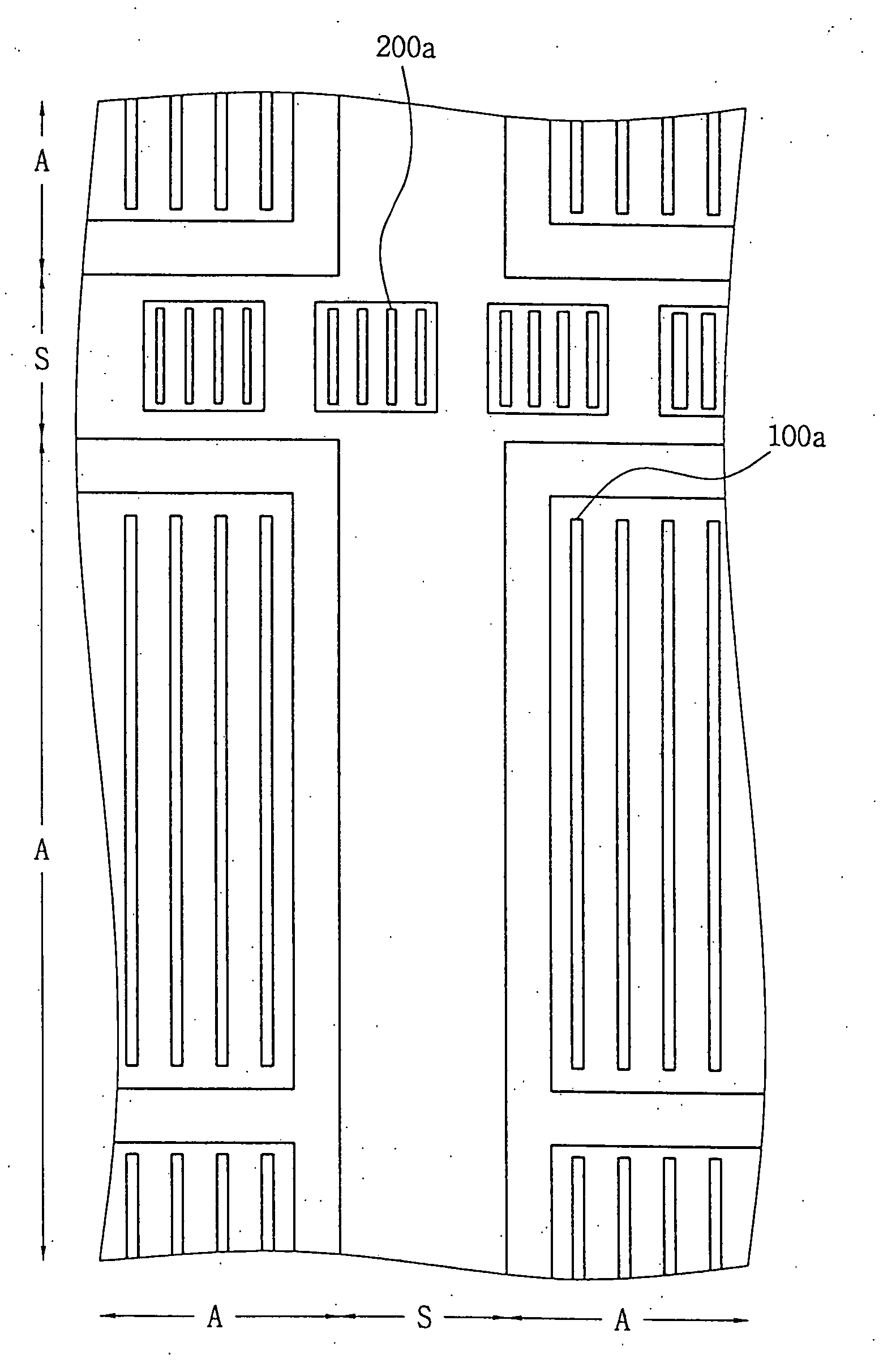
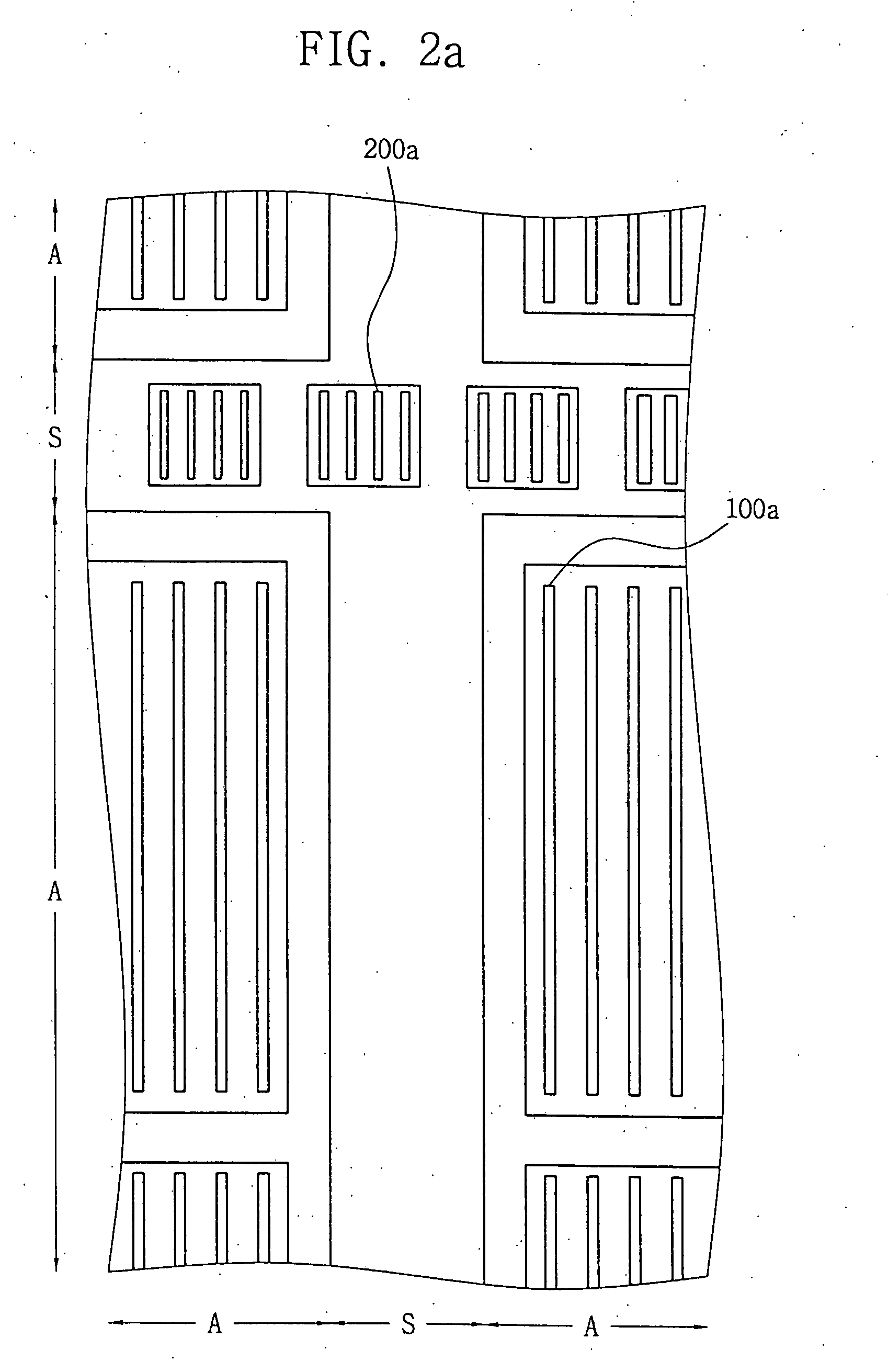
[0036] A photoresist pattern of the present invention, as shown in FIG. 2a or 2b, includes main patterns 100a or 100b in device-forming regions A defined on a semiconductor substrate, and a plurality of test patterns 200a or 200b in scribe regions S, wherein the scribe regions S separate the device-forming regions A from one another. The main patterns 100a or 100b have a given critical dimension. The openings of the test patterns 200a or 200b have shapes identical to those of the main patterns 100a and 100b and have critical dimensions different from each other. As will be described below, the test patterns 100a or 100b are dedicated for use in determining whether a defect had occurred in reflowing the photoresist to form the main patterns 100a or 100b.

[0037] The main patterns may be in the form of patterns 100a of lines and spaces (FIG. 2a) for use in forming line...


PUM

PropertyMeasurementUnit
temperatureaaaaaaaaaa

Abstract

A photoresist pattern and a method of fabricating the same make it easy to quickly identify a particular portion of a photolithography process that is responsible for causing process defects. The method of fabricating the photoresist pattern includes forming main patterns having a predetermined critical dimension in device-forming regions of a semiconductor substrate, and forming a plurality of test patterns in scribe regions of the substrate. The scribe regions are defined alongside the device-forming regions and separate the device-forming regions from one another. The test patterns have shapes similar to that of the main patterns. Also, one of the test patterns has a critical dimensions similar to that of the main patterns, and other test patterns have respective critical dimensions that are different from the critical dimension of the main patterns.

Description

BACKGROUND OF THE INVENTION [0001] 1. Field of the Invention [0002] The present invention relates to a method of fabricating semiconductor devices. More particularly, the present invention relates to a photolithographic process of fabricating a photoresist pattern, and to the quality control of such a process. [0003] 2. Description of the Related Art [0004] Semiconductor devices are dramatically evolving in conjunction with rapid developments in the fields of data communications and data processing. In these fields, especially, semiconductor devices must operate at high speeds and at the same time to have a large storage capacity. In response to these requirements, techniques of fabricating semiconductor devices are being studied and developed with the aim of maximizing the integration, reliability, response speed, etc., of the devices. [0005] The fabricating of semiconductor devices typically includes a deposition process of forming a target film on a semiconductor substrate, a pho...

Claims


Application Information

Patent Timeline
Patent Type & Authority Applications(United States)
IPC IPC(8): H01L21/027G03F1/14G03F7/20H01L21/66H01L23/544
CPCG03F1/14G03F1/44Y10S438/942G03F7/7065H01L22/34G03F7/70625G03F1/36G03F1/62H01L21/76802
Inventor CHOI, YEON-DONGBAEK, KYOUNG-YUN
Owner SAMSUNG ELECTRONICS CO LTD
Why Eureka
Try Eureka